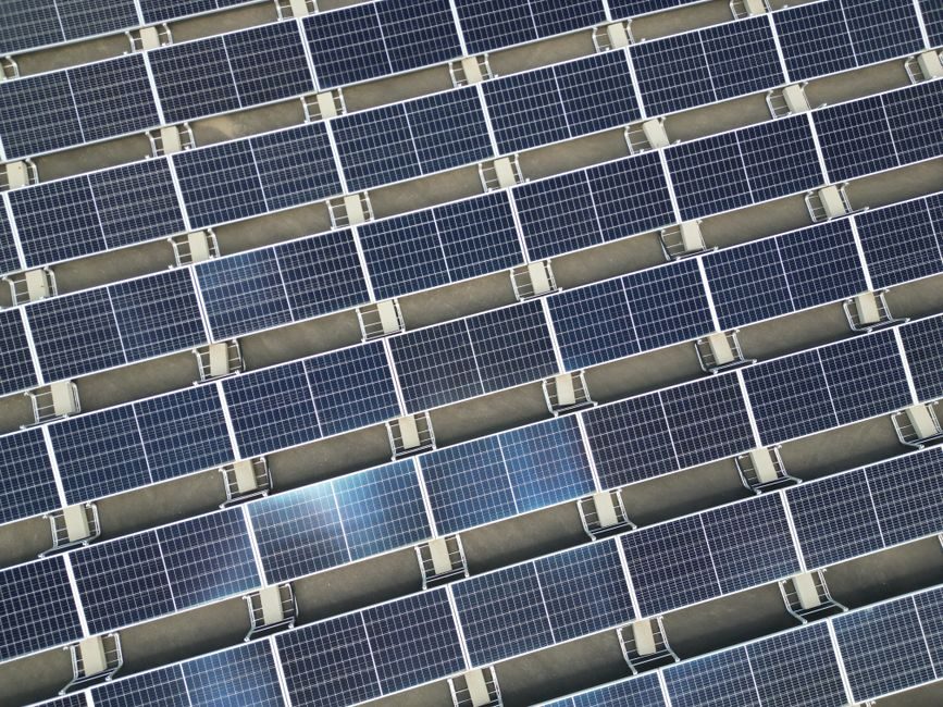
By the end of 2023, total global silicon-wafer production capacity reached about 974.2 GW, up 46.7% year-on-year, while 2023 wafer output was approximately 681.5 GW, up 78.8% year-on-year [S2].
Country-level capacity is heavily skewed: the top-five producers — concentrated in mainland China, Taiwan, Japan, South Korea and Germany — historically account for the overwhelming majority of merchant wafer output, and Chinese PV-wafer lines alone now operate on multi-hundred-GW nameplates, while Chinese silicon-carbide (SiC) wafer capacity is projected to capture about 50% of the global SiC substrate share by 2024 [S4].
Country-by-Country Capacity Map: Who Actually Makes the Wafers
The country split is bimodal: PV/mono wafers are essentially a Chinese story, while semiconductor-grade polished wafers (150/200/300 mm) remain a Japan/Taiwan/Germany/South Korea story. Okmetic's Finland site focuses on crystal growth plus 150-200 mm wafers, and the 200 mm fab expansion announced by the company will more than double its 200 mm output [S5]; that single-site line is dwarfed by Chinese PV-wafer nameplates measured in tens of GW each.
For semiconductor wafers, Shin-Etsu Chemical and Sumco (Japan), GlobalWafers (Taiwan), Siltronic (Germany) and SK Siltron (South Korea) collectively control the bulk of merchant 300 mm supply; their capacity additions are lumpy, tied to TSMC, Samsung and Intel node ramps. Chinese merchant 200/300 mm capacity at NSIG, Simgui and Zingsemi has grown in 2023-2026 but still trails in the most advanced nodes, with the gap being capability (epitaxy, low-defect polished wafer) rather than raw square-metre output.
PV-wafer capacity is a different league. Chinese PV-wafer producers (LONGi, TCL Zhonghuan, GCL, Shuangliang/Double-Listed Shuangliang节能) each run 50-150 GW-scale nameplates. Shuangliang节能 reported Q3 2023 revenue of 6.659 billion yuan (+49.68% YoY) and net profit of 785 million yuan (+64.61% YoY), with 20.44% gross margin and 12.31% net margin as silicon-wafer shipments rebounded and line operating rates recovered [S3] — a snapshot of how rapidly Chinese PV-wafer cashflows turn when utilisation climbs.
What Changed in the Last 6 Months (Jan 2026 – Jul 2026)
The most concrete data point inside the research window is Okmetic's 200 mm fab expansion in Finland, disclosed on 2026-06-09, which will more than double the company's 200 mm output at its Vantaa site once fully ramped [S5]. For Chinese PV-wafer producers, the 46.7% YoY capacity expansion reported for 2023 [S2] has not been matched by an equivalent nameplate build-out in 2024-2026, but operating rates have tightened as inventory normalised and TOPCon/HJT demand pulled mono-wafer volumes back into the 70-80% utilisation range.
For comparison, a parallel global-capacity map for steel global production capacity by country shows a similar pattern — concentrated Asian supply, narrower European specialty share — which mirrors how silicon-wafer supply also splits into commodity-PV (China-dominant) and specialty-semiconductor (Japan/Taiwan/Germany) tiers. Buyers who treat "silicon wafer" as one product usually mis-spec the line they are quoting; treat PV-mono and semiconductor-grade polished wafers as two separate sourcing problems.
Selection Criteria by Application
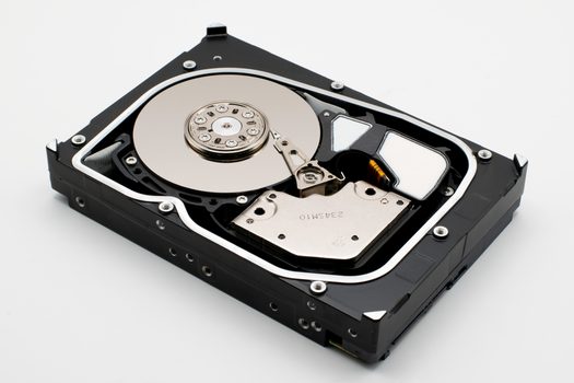
PV mono-wafer buyers should track: (1) wafer type — p-type PERC vs n-type TOPCon vs HJT, with resistivity and lifetime specs shifting by cell technology; (2) thickness trend — 150 µm in 2023 → 130 µm and below for TOPCon/HJT, with Tairyo Pro and similar thin-wafer lines gaining share; (3) wafer dimension — G12 (210 mm) vs M10 (182 mm) format wars, with the G12 share continuing to grow on per-watt capex logic; (4) polysilicon-price pass-through, which is the single largest cost driver. [S1]
Semiconductor-wafer buyers (foundry, MEMS, power) should track: (1) diameter — 200 mm vs 300 mm, with 300 mm roughly 2.25× the area per wafer and the cost-per-die king; (2) crystal growth method — Czochralski (CZ), Magnetic-Czochralski (MCZ), or Float-Zone (FZ), with FZ commanding a premium for power devices; (3) doping and resistivity window, which gate IGBT vs MOSFET vs diode designs; (4) surface finish — polished, epitaxial-ready, or epi wafer, which is where silicon carbide and silicon nitride substrate alternatives come in for high-voltage, high-temperature designs.
SiC and SiN as Adjacent Substrate Plays
For 1200 V+ traction, 1700 V+ industrial drives, and 3.3 kV+ grid applications, silicon gives way to silicon carbide substrates. SICC (天岳先进), TanKeBlue (天科合达) and Sanan Optoelectronics (三安光电) have all invested heavily in 150 mm SiC wafer expansion, with Chinese SiC capacity projected to hit about 50% of global SiC substrate share by 2024 [S4] — a notable contrast to the silicon-wafer market, where Chinese share in advanced-node semiconductor-grade wafers remains a minority position.
For MEMS, RF and high-reliability hermetic packages, silicon nitride layers (low-pressure CVD SiN, stoichiometric Si3N4) are deposited on silicon handle wafers rather than used as the substrate itself, but the wafer's flatness, bow and TTV (total thickness variation) still gate yield — buyers who ask for "any 200 mm wafer" without TTV ≤ 5 µm and bow ≤ 30 µm often discover the problem at dicing, not at incoming inspection.
Limits, Failure Modes and Common Mis-Specs
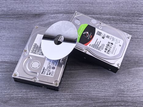
Chinese merchant-wafer lines remain fully booked multiple quarters out even when global nameplate capacity grows; in Q2 2021 every major Chinese wafer maker was already sold out, and imports still had to fill the gap [S6]. That book structure has not materially loosened in 2024-2026, so a buyer who plans to "qualify a Chinese source when convenient" will find the convenience window is about 18-24 months long and tied to a specific node.
Sourcing Standards and What to Put on the PO
For semiconductor wafers, specify per SEMI standards (M1 for 300 mm notch/flat, M11 for wafer dimension, M1-0302 for edge profile, plus customer-specific defect/particle limits). For PV wafers, the spec baseline is China Photovoltaic Industry Association (CPIA) and SEMI PV-grade standards, with thickness tolerance typically ±10 µm and TTV ≤ 20 µm for TOPCon/HJT. For SiC substrates, the binding specs are micropipe density (target ≤ 1 cm⁻²), wafer bow (≤ 25 µm for 150 mm), and basal plane dislocation (BPD) density — these are the three parameters that gate yield at the epitaxy step. [S2]
Resistivity window: CZ p-type 1-100 Ω·cm for most logic and memory; FZ n-type 100-1000 Ω·cm for power devices; MCZ p-type for IGBT substrates. None of these are negotiable in the PO — a 0.5 Ω·cm wafer in a 10 Ω·cm IGBT line is a field failure, not a yield problem. This is also why pressure transmitter and flow meter buyers on PV lines need to track wafer-thickness tolerances in their spec package: thinner wafers change the in-line stress and the calibration constants of the inline measurement cells.
2026 Buying Window: Where the Spreads Are
For 300 mm polished wafers, the capacity expansion window is gated by GlobalWafers' (Taiwan/Singapore/Italy) and Siltronic's (Germany/Singapore) fab schedules, plus Shin-Etsu's日本 expansion — these are 24-36 month build-outs, not quarterly swings, so 2026 contract pricing is set against 2024-2025 polysilicon cost curves, not spot. Buyers who locked 12-month wafer supply at end-2025 are paying 2025 prices; those re-quoting in 2026 are seeing mid-single-digit increases on long-term agreement volumes.
Trackable signals for the next quarter: (1) Okmetic's 200 mm Vantaa line tool-in dates, which set the European 200 mm supply ceiling for 2026-2027 [S5]; (2) Chinese SiC substrate shipments from SICC and TanKeBlue, which validate whether the 50% global share target [S4] is met or slipped; (3) GlobalWafers' Dresden fab output, which is the largest 300 mm greenfield in Europe and a key signal for whether the EU Chips Act capacity is actually landing on schedule.