
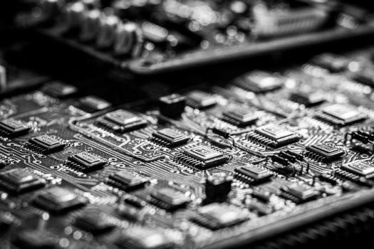
Polished monocrystalline silicon wafers traded between US$10 and US$100 per piece at 25-piece minimum order quantity on Made-in-China listings dated 2026-06-02, with both P-type and N-type 12-inch product cards pointing to Fine Silicon Manufacturing (Shanghai) Ltd. as an audited supplier [S3]. The same supplier surface also shows custom 12-inch semiconductor wafer lines that the listing language tags as "Best Price for Semiconductor Silicon Wafer", a positioning that sits next to — not above — dedicated 6-inch, 8-inch and prime-grade alternatives on the directory [S5].
The pricing spread on 2026-06-02 listings is wide enough to drive engineers straight to a spec sheet: US$10 floor typically maps to test-grade, dummy-grade or reclaim wafers, while US$100 ceiling lines up with prime monocrystalline product where surface roughness, TTV and metal-contamination budgets match the device fab's incoming-material spec [S3][S5]. For process engineers sourcing across diameters, the practical decision on 2026-06-26 is diameter first (6/8/12 in.), grade second (prime/test/dummy), and lot-size/lead-time third — not raw unit price.
Price bands on 2026-06-02 Chinese B2B listings
Monocrystalline wafer listings published on 2026-06-02 sit in a US$10–100 per piece band with a 25-piece MOQ, and the same price card is repeated for both P-type and N-type 12-inch entries from Fine Silicon Manufacturing (Shanghai) Ltd., a Gold Member and Audited Supplier on Made-in-China [S3]. A parallel "Silicon Wafer Process Price" page dated 2026-06-06 carries the identical US$10–100 / 25-pc MOQ format for the same audited supplier, confirming that this is the live spot-quote band rather than a single ad [S5]. Sourcing against a US$0.40–4.00 per square-inch equivalent at 12 in. (≈ 100 mm equivalent in area terms) is the kind of back-of-envelope floor an engineer should run before opening a bank inquiry.
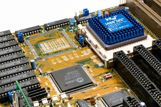
Test/dummy wafer lines listed on Fine Silicon Manufacturing's parent site (FSM, Shanghai) include thermal-oxide, PETEOS, nitride, POLY, Cu, W, TiN, TaN and PR pattern-wafer customization, with the company's published footprint at 1,200 m² and team-experience claims of more than 5 years. For a fab equipment-engineer, the takeaway is that the same Chinese vendor cluster will quote both prime 12 in. and the consumable test/dummy wafer stack — and the consumable side is where the industrial machinery, parts and raw materials ecosystem for nitride-coated monitor wafers is anchored.
Diameter and grade: the spec that actually moves unit price
Sourcing pages dated 2026-06-02 and 2026-06-06 use 12-inch (300 mm) terminology for the headline "Best Price" SKU, which is consistent with mainstream logic and memory fabs that have standardized on 300 mm since the 2000s node transition [S3][S5]. Legacy 6-inch (150 mm) and 8-inch (200 mm) lines for analog, MEMS and power-device fabs typically run below the 12-inch price ceiling, but the Made-in-China spot listings on 2026-06-02 do not show separate 6/8 in. price cards on the same query — a sourcing-engineer flag that diameter choice needs to be confirmed with the supplier directly [S3].
Grade drives the spread within the same diameter: prime wafer pricing sits at the upper end, test and dummy wafer SKUs at the lower end, and reclaim wafers — polished and re-used for non-production monitor and equipment-qualification work — sit at the floor. The Polishing Corporation of America homepage, accessed on 2026-06-24, advertises a "Wafer Reclaim" service line covering wafer stripping, polishing and reclaim for customers who want to keep monitor and qualification wafers inside a closed loop [S1]. A typical reclaim spec targets surface metal contamination, particles and roughness restored to a usable spec rather than to prime, which is why reclaim is a parallel procurement lane and not a substitute for prime wafer offtake.
Reclaim, test, and dummy: where US$10 floor wafers actually go
Polishing Corporation of America describes a reclaim flow that takes customer-used wafers through stripping, re-polishing and surface-prep stages to return them to a monitor-wafer spec, and the company frames the service as a continuous loop for fabs that burn monitor wafer inventory on every tool-qualification run [S1]. Pricing for the reclaim service is not published on the company homepage captured on 2026-06-24, so an engineer evaluating reclaim vs. virgin test wafer has to request quote on a wafer-count or monthly-volume basis [S1].
FSM (Shanghai) — the same vendor surface behind the Made-in-China 12-inch spot cards — also lists dedicated test/dummy and film-coating customization on its 2026-06-25 homepage, covering thermal oxide, PETEOS, nitride, polysilicon, Cu, W, TiN, TaN, PR and pattern-wafer stacks. For buyers building a monitor-wafer pool, the decision between a US$10 dummy wafer and a reclaimed monitor wafer turns on what the downstream tool's qualification recipe measures: metal and particle counts favour fresh test-grade silicon, while mechanical-handling and OES/SECS/GEM dry-run checks are comfortable on a reclaim or dummy lot. The same vendor cluster bridges silicon carbide and SiC wafer SKUs to silicon monitor wafers, which matters for compound-semiconductor lines running SiC monitor alongside Si production.
How the 2015 SEMI baseline maps onto 2026 sourcing
Daedal Research's 2018-2022 forecast, summarized via PRLog in 2022, framed the global silicon-wafer market by value across APAC and North America with no specific 2026 dollar figure in the visible text [S4]. That means an engineer reading the 2026-06-02 spot listings has to use 2015 area data as the only quantitative anchor from the research material, and accept the unit ASP as a derived band from the live spot quote [S2][S3].
The 2015 SEMI line of "10,434 MSI ≈ 6,500–6,800 k wafer-equivalents at 12-inch equivalent" (back-of-envelope: 10,434 MSI / ~1.55 in.² per mm² of effective area per 12 in. wafer) is a useful magnitude check against current Chinese supplier capacity, not a current shipment figure [S2]. For a foundry procurement engineer, the 2026-06-26 read is that the SEMI 2015 anchor still holds as an order-of-magnitude benchmark, while spot pricing on 2026-06-02 has compressed into a tight US$10–100 / 25-pc MOQ band on the same Chinese vendor surface [S2][S3].
Decision grid: 12-inch prime vs 12-inch test vs 6/8-inch legacy vs reclaim
A spec-first comparison for an engineer opening a quote on 2026-06-26: (a) 12-inch prime monocrystalline silicon sits at the top of the US$10–100 spot band, the only listing tier on the 2026-06-02 Made-in-China card flagged as a 12-inch N-type/P-type "Best Price" SKU from an Audited Supplier [S3]; (b) 12-inch test/dummy SKUs share the same vendor surface (FSM) with thermal-oxide, PETEOS, nitride, POLY, Cu, W, TiN, TaN, PR and pattern-wafer customization options on the 2026-06-25 homepage; (c) 6-inch and 8-inch lines are absent from the visible spot-card set on 2026-06-02 / 2026-06-06, so diameter confirmation must be requested; (d) reclaim wafer pricing is unpublished on the PCA homepage captured 2026-06-24 and is quote-only [S1][S3].
The two material cross-references that actually pay off in a silicon-wafer spec doc are silicon carbide for compound-semiconductor power-device lines that pair Si monitor wafers with SiC monitor SKUs from the same vendor cluster, and silicon nitride for the nitride-coated monitor and film-wafer stack that the FSM homepage lists on 2026-06-25. Where the same engineer might also touch silicon steel is at the grain-oriented electrical-steel side of the broader silicon materials market — a different spec envelope (magnetic flux density, lamination thickness) and a different vendor pool, but a useful reminder that "silicon wafer" search results will span both semiconductor and electrical-steel SKUs.
Sourcing risk: vendor concentration, MOQ and audit depth
The 2026-06-02 spot cards repeatedly name Fine Silicon Manufacturing (Shanghai) Ltd. as the supplier, with a Gold Member and Audited Supplier tag — a positive procurement signal but also a single-supplier concentration risk for buyers locking in 12-inch volume on 25-pc MOQ [S3]. The 2026-06-06 "Silicon Wafer Process Price" page mirrors the same supplier and price band, which is a useful cross-check that the US$10–100 floor is not an isolated listing anomaly [S5]. Continental Device India Ltd. also surfaces a "Silicon Wafer" product card on HKTDC sourcing dated 2026-03-28, although the visible card text is fragmentary and does not show price or MOQ — a flag for engineers to treat this as a discovery listing rather than a quotable offer [S6].
For risk control, the practical move on 2026-06-26 is to (i) request a written spec sheet (diameter, grade, orientation, resistivity, TTV, bow/warp, surface metal budget) from any vendor quoting the US$10–100 band; (ii) qualify a second source outside the Shanghai cluster to avoid a single-region logistics shock; (iii) run a reclaim pilot with a US-domiciled reclaimer (PCA, per its 2026-06-24 homepage) for monitor-wafer consumption above a fab-defined break-even lot size [S1][S3]. A reader cross-checking this against broader industrial-spec material will see the same single-supplier concentration pattern we cover in Rare Earth Upstream and Downstream Industries: 2026 Supply Chain Map and the spec-first comparison framing in Top Steel Companies 2026: Spec Map for B2B Buyers and Engineers — both of which apply the same audit, MOQ and second-source gates to upstream silicon raw materials.
Track three signals after 2026-06-26: the next SEMI SMG annual area-shipment release (last visible anchor: 10,434 MSI for 2015 [S2]); any update to the Fine Silicon Manufacturing 12-inch "Best Price" SKU on Made-in-China; and a published reclaim-service price card from PCA, which would convert the 2026-06-24 quote-only flow into a real procurement benchmark.