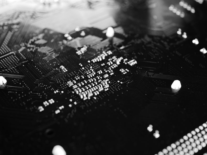
SiBranch Microelectronics, founded 2006 in Ningbo, is one of the merchant CZ/FZ silicon and compound-wafer sources active on B2B platforms as of 2026-06-26, offering semiconductor-grade wafers alongside engineering substrates [S1]. Across the same platforms, Shanghai Panmeng Electronic Materials Co., Ltd. (Songjiang, Shanghai) lists CZ and FZ silicon wafer plus silicon ingot as main products, reflecting the standard Chinese merchant-wafer profile: ingot pull, wafer slice, edge-grind, polish [S10].
Go4WorldBusiness lists bulk silicon-wafer offers at US$350–$2,500 per piece on CIF terms, covering Prime, Test, Monitor, SEMI-standard and customized diameters from 2-inch up through 300 mm, plus Silicon-On-Insulator (SOI) variants [S6]. HKTDC's Sourcing portal also surfaces Continental Device India Ltd. as a registered silicon-wafer supplier, evidence that India is now visible on the merchant-wafer map [S7]. Alibaba's "silicon carbide wafer" supplier page lists factories with response rates of 82.1% and 92.3%, with domestic-market and Western Europe among the top shipment corridors [S2].
Merchant-Wafer Tiers: What the 2026 Supplier Map Looks Like
Three tiers are visible in the 2026 supplier set. Tier 1 covers integrated device manufacturers running captive fabs (Intel, Samsung, TSMC, SK Siltron, GlobalWafers, SUMCO, Siltronic) — these rarely appear on B2B marketplaces and instead move wafer via long-term agreements. Tier 2 is merchant CZ/FZ producers serving external fabs: Shanghai Panmeng (CZ + FZ, China) [S10] and SiBranch (Ningbo, multi-material) [S1] sit here, with the Jiangyin/Songjiang/Shanghai cluster as the most active Chinese node.
Specialty substrates form a parallel track. Alibaba's compound-wafer page is dominated by silicon carbide (SiC), silicon nitride-bonded SiC (SiSiC), reaction-bonded SiC (RBSiC/SiSiC), sintered SiC and recrystallized SiC, plus alumina, zirconia and aluminium-nitride ceramics — all of which overlap with the silicon carbide and silicon nitride ceramic families used in wafer-handling and furnace furniture, not just in power-device epi substrates [S2].
Diameter, Spec and Tolerance Bands the Buyer Should Anchor On
The 2026 mainstream diameters for prime-grade silicon are 150 mm (6"), 200 mm (8") and 300 mm (12"); 2" through 100 mm remain standard for MEMS, RF and power-discrete lines, and go4worldbusiness lists the full 2-inch to 300 mm spread under one supplier SKU [S6]. SEMI standards (SEMI M1 for wafer dimensions, SEMI MF for flat/notch, SEMI M44 for resistivity) are the universal procurement language — PCA flags SEMI-standard compliance as the baseline for its reclaim output [S9].
For solar mono wafers, Okorder's 156×156 mm mono P-type wafer listing quotes 156×156 ±0.5 mm and below as the conventional crystalline-Si solar cell raw form factor [S4]. Okorder also lists "Solar Mono Silicon Wafer Amorphous Silicon Dice Specification 2" as a 2026 product reference, pointing at the diced/specialty cut end of the silicon-wafer market rather than prime wafer [S3]. Go4WorldBusiness's Jinglong Industry & Commerce Group offering is similarly PV-oriented, with surface-quality tuned to "the updating request of PV development" rather than semiconductor fab rules [S5].
Selection Criteria: Prime vs Test vs Reclaim vs Compound
Prime wafers are the unscratched, particle-controlled substrates that go directly into active device fabs. Test and monitor wafers are used for process-tool qualification and particle/etch-rate monitoring — go4worldbusiness's listing explicitly enumerates Prime, Test, Monitor, SEMI-standard and customized categories as separate SKUs [S6]. Reclaim wafers are customer-owned wafers that have been stripped, cleaned and re-polished: PCA's 12-hour in-house reclaim cycle (stripping, cleaning, reclaim, thin films, inspection) is the operational benchmark for US-based buyers [S9]. Compound-semiconductor wafers (SiC, GaN, InP) sit in a separate spec regime governed by the wafer-substrate producers active on Alibaba's compound-ceramic page [S2].
Key decision criteria a process engineer should weigh: (1) diameter and SEMI-standard compliance, (2) crystal growth method (CZ vs FZ — FZ has higher resistivity and lower oxygen, used for power devices and rad-hard; CZ is the default for logic/memory), (3) dopant type and resistivity range, (4) surface finish (prime polished, etched, epitaxial-ready), (5) flat/notch orientation, (6) TTV / bow / warp and particle adders, (7) lead time and minimum order quantity. Shanghai Panmeng's dual CZ + FZ positioning is the merchant-wafer equivalent of a "covers both" catalog [S10]; SiBranch goes wider, mixing semiconductor wafers with compound-semiconductor substrates under one roof [S1].
Geographic Sourcing Patterns and Trade Corridors
China is the dominant origin node in the 2026 supplier set. Of the merchant-wafer manufacturers visible on Made-in-China and Alibaba, Shanghai and the Yangtze River Delta (Songjiang, Jiangyin, Ningbo) form the densest cluster [S1][S10]. Alibaba's silicon-carbide wafer export split, drawn from 2026 supplier data, shows domestic market 15–55% (depending on the supplier), Western Europe 15–25% and Southeast Asia ~10% as the leading outbound corridors [S2].
Outside China, US reclaim and specialty houses are anchored in the Northeast (Polishing Corporation of America, plus a New Jersey-based go4worldbusiness supplier covering 2-inch to 300 mm) [S6][S9]. India now appears on HKTDC's supplier index via Continental Device India Ltd., though its wafer offerings currently read more like trading than captive CZ pull [S7]. European and Japanese merchant wafer majors (Siltronic, SUMCO, GlobalWafers, Soitec for SOI) are largely absent from B2B marketplaces in this 2026 snapshot, which is consistent with their fab-direct commercial model.
MOQ, Price Bands and Sourcing Risk
For small-quantity engineering and R&D buyers, the go4worldbusiness Prime/Test/Monitor listing prices wafers at US$350–$2,500 per piece on CIF terms, with MOQ left as "Not Specified" — typical of the low-volume, mixed-diameter trading model [S6]. On Made-in-China, etching-wafer lines open at US$100,000 per piece with a 1-piece MOQ for capital-equipment-adjacent items, and 2-inch PFA wafer cassettes/clamp fabricators advertise factory-direct sales with corrosion-resistant customization for semiconductor wet-process use [S8]. For solar mono wafers, the Okorder 156×156 mm listing is positioned as a raw-material SKD-style buy, not a high-volume fab contract [S4].
Procurement risk in 2026 sits in three places. First, spec mismatch — the same SKU may be sold as "SEMI standard" without a cited SEMI M-revision, and the buyer should ask for the actual M1/MF/M44 revision. Second, dual-use ambiguity — a "silicon wafer" listing on Alibaba or Made-in-China may be a metallurgical-grade or solar-grade blank, not prime semiconductor wafer, and price is the first tell. Third, lead-time risk for FZ and large-diameter CZ, where merchant capacity is tight. For buyers coupling wafers to downstream ceramics like silicon nitride wafer-handling fixtures or silicon steel process tooling, the relevant companion-supplier question is whether the wafer and the ceramic-fixture vendor share a port — Shanghai/Ningbo clusters make that easy [S1][S2].
How the 2026 List Maps to a Real Sourcing Path
A pragmatic 2026 sourcing path looks like this: for prime 200/300 mm logic-grade silicon, engage the merchant majors directly (off-platform); for small-lot engineering and 2–6" substrates, the go4worldbusiness and Made-in-China channels (Shanghai Panmeng, SiBranch, the New Jersey trading house) cover it [S6][S1][S10]; for reclaim and test wafers, US-based PCA is the visible benchmark with 12-hour reclaim turnaround [S9]; for SiC and other compound substrates, Alibaba's factory cluster with 82–92% response rates is the working channel [S2]; for solar-grade mono, Okorder's 156×156 mm P-type offering is the reference SKU [S4].
Adjacent-process buyers looking at high-purity upstream silicon will recognise a structural parallel in Copper Supply Shortage 2026: Risk Vectors and Mitigation Levers — the same spec-trap pattern (claimed grade vs verified grade, captive vs merchant, regional cluster vs import-dependent node) shows up in metallurgical silicon for PV and electronics, which is why a tier-aware supplier map matters more than a long list.
Closing signals to track over the next quarter: (1) whether more Chinese CZ/FZ merchant houses move onto B2B platforms with published SEMI M1/MF/M44 compliance statements — Shanghai Panmeng and SiBranch are the early indicators [S1][S10]; (2) whether PCA-style reclaim providers expand diameter coverage above 300 mm as legacy 200 mm lines age [S9]; (3) whether India-listed wafer suppliers (Continental Device India Ltd. on HKTDC) move from trading to captive CZ pull [S7]. Each of these would shift the 2026 sourcing map more visibly than a new trading-house listing.