A 1 kW/m² terrestrial AM1.5 reference irradiance defines the power-density target every commercial photovoltaic module is rated against, and the cell-to-module pipeline is engineered to harvest that flux with as little optical and resistive loss as possible [S1].
The industrial chain splits cleanly into upstream cell fab (mono- or multi-crystalline silicon, p-type PERC or n-type TOPCon/HJT) and downstream module assembly (stringing, lay-up, lamination, framing), with every major Indian tier-1 line audited in 2026 publicly stating 100% pre- and post-lamination EL plus AOI inspection as a baseline acceptance gate [S4][S5][S7].
Upstream Cell Fabrication: From Wafer to Contacted Cell
The cell-fab sequence for a p-type PERC line begins with saw-damage etch and alkaline texturing of a Czochralski monocrystalline wafer, which produces the random-pyramid surface that traps light by total internal reflection; saw-damage removal typically removes 5–10 µm per side before texturing is applied [S6].
After cleaning, an n+ emitter is formed by POCl3 tube-furnace diffusion at roughly 800–850 °C, the resulting phosphosilicate glass is stripped in dilute HF, and a SiNx anti-reflection coating is deposited by PECVD to a thickness tuned to a quarter-wavelength at the cell's target absorption peak [S6]. A rear-side stack — laser- or chemically opened local BSF contacts plus an AlOx/SiNx passivation layer — defines the PERC architecture that displaced standard aluminum-back-surface-field cells through the late 2010s.
Front-side metallization is screen-printed Ag paste, dried, then co-fired in a belt furnace so the paste fires through the SiNx to form a front contact while the rear Al layer alloys to the silicon [S6]. For n-type TOPCon lines — the architecture now advertised as the leading single-junction technology — the front side mirrors a PERC line, but the rear is rebuilt with an ultrathin tunnel-oxide (~1.5–2 nm) plus a thin polycrystalline silicon layer deposited by LPCVD or PECVD, which is what unlocks the higher Voc that TOPCon vendors cite in their 2026 marketing collateral [S4]. Module makers still running n-type HJT add a passivating intrinsic a-Si:H stack on both sides and plate the TCO with a low-temperature silver or copper seed layer.
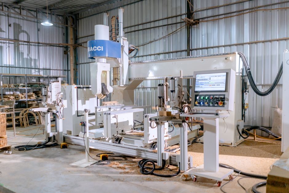
Module Assembly: Lay-up, Lamination and Framing
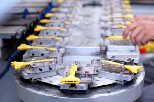
Cell-to-module conversion starts with laser or thermal singulation, after which cells are sorted by power bin; the modern half-cut architecture — typically 108 or 144 half-cells in a residential/commercial panel — needs a tabber-and-stringer that solders 8–12 ribbons per cell string with a cell-gap tolerance normally held below ±0.5 mm [S9].
Once stringed, the stack-up is glass → EVA (typically fast-cure, ~0.45 mm) → cell matrix → EVA → backsheet (or a second glass for bifacial glass-glass modules), with the junction box pre-positioned and potted before the pack enters the laminator [S6]. Vacuum lamination is the thermal bottleneck: the chamber is evacuated to remove trapped air, then heated to roughly 140–155 °C for 12–20 minutes so the EVA crosslinks and bonds the stack into a single optical-mechanical unit, after which the panel is cooled under restraint to prevent delamination [S6]. Aluminum framing, silicone edge-sealant dispense, and junction-box potting complete the BOM before the module reaches the flash tester.
For lines flagged as glass-glass bifacial, the backsheet is replaced by a second 2.0 mm tempered glass and the EVA is often swapped for a higher-crosslink-density POE to block moisture ingress over the 30-year power warranty the 2026 tier-1 datasheets are now quoting [S4].
Process Support Systems: Wet Benches, Wastewater and Exhaust
PV fab is wet-heavy, and the auxiliary process support package is sized by the chemical throughput of the diffusion, etch, and texturing baths. Acidic and alkaline waste streams are segregated: HF-bearing streams from SiNx and PSG strip are routed to a calcium- or aluminum-neutralization stage to drop fluoride below the discharge limit, while IPA-bearing texturing rinses are recovered or sent to a dedicated organics treatment skid [S8].
Exhaust treatment is dominated by POCl3, NOx, SiH4, NH3 and HF, so a typical cell line pairs a local scrubber bank on each tool with a central packed-tower wet scrubber for the bulk acid gases, plus thermal oxidation for the silane streams used in the PECVD and TOPCon LPCVD stations [S8]. Ultra-pure water systems feed the rinsing and the final surface-clean steps, with resistivity normally held above 15–18 MΩ·cm to keep the post-texture surface clean enough for the SiNx PECVD step to deposit a defect-free film.
Facilities that move from p-PERC to n-type TOPCon have to add silane/nitrogen bulk-gas distribution, an LPCVD hot-wall furnace cluster, and an HF-last clean sequence for tunnel-oxide integrity — which is why the 2026 capex announcements from Indian manufacturers cluster around TOPCon retrofits rather than greenfield PERC [S4][S5].
Inline Quality Control: EL, AOI and Flash Test
100% pre-lamination and 100% post-lamination electroluminescence imaging is now table stakes for tier-1 lines, and the same lines pair EL with automated optical inspection cameras looking for cell cracks, ribbon misalignment, and solder defects before the module is framed [S5].
EL works by forward-biasing the cell string at the rated short-circuit equivalent and imaging the radiative recombination: any microcrack, broken finger, or disconnected cell shows up as a dark area in the captured image, which is the reason pre-lamination EL is used to catch tab-wire bonding errors before EVA crosslinks them in [S5]. AOI complements EL by checking the geometric stack-up — cell spacing, ribbon overlap, junction-box alignment, and backsheet/glass cleanliness — at line speed.
Final electrical test is a flash test to a class-A or class-AAA pulsed solar simulator at STC (1000 W/m², AM1.5G, 25 °C cell), which reports Pmax, Voc, Isc, fill factor, and the temperature coefficients; bifacial modules are also gain-tested under rear-side irradiance per the IEC 60904-1-2 bifaciality method that most 2026 datasheets cite [S4][S7]. Inline IV at the tabber-stringer is increasingly added so that under-performing cells are binned out before they reach lay-up, which is where the half-cut topology starts to show its yield advantage over full-cell layouts.
Cell Architectures Compared: PERC, TOPCon and HJT
PERC remains the high-volume incumbent with a mature supply chain, TOPCon is the 2026 expansion default because of its higher bifaciality and slightly better temperature coefficient, and HJT is the option with the highest demonstrated efficiencies but the most demanding low-temperature process window. Aluminum frames and the lamination process are largely common across all three, but the cell string, the BOM per cell, and the Ag paste consumption per watt differ markedly — TOPCon cuts the front-side Ag loading versus PERC, while HJT can drop to zero front-side Ag with copper plating if the line is built for it. [S1]
Module wattages follow a similar step: a 144-half-cell mono-PERC residential panel sits in the 540–570 W range, a TOPCon equivalent moves into the 560–610 W band, and an HJT panel of the same cell count is typically quoted 10–30 W higher with a tighter Voc tolerance and a lower temperature coefficient around –0.24 %/°C versus –0.35 %/°C for standard PERC [S4][S7]. This is also why TOPCon producers in 2026 are reporting 11 GW-scale single-site capacities rather than the 1–2 GW PERC lines of five years ago — the per-line throughput of the cell-fab bottleneck tools, and the inline EL/AOI envelope around them, scale with the wafer format rather than the cell chemistry [S4].
For comparison, the selection criteria that matter most in 2026 module procurement are: bifaciality gain (typically 5–25% depending on ground albedo), temperature coefficient (–0.30 to –0.24 %/°C across the three architectures), annual degradation rate (0.40–0.55 %/yr tier-1 warranty), and mechanical load rating (2400 Pa snow / 5400 Pa wind uplift on the datasheets of multiple Indian tier-1 brands) [S4][S7]. Procurement teams that weight degradation and temperature-coefficient performance more than sticker price consistently land on TOPCon; teams that weight lowest $/W above all else still see PERC on allocation.
Use Cases, Limits and Where the Process Breaks
The dominant use cases for the resulting modules — utility-scale ground-mount, commercial rooftop, residential rooftop, and increasingly agrivoltaic — all share the same cell and module BOM, but the framing, glass thickness, and backsheet choice vary: 3.2 mm front glass is the residential default, dual 2.0 mm glass-glass is the utility/bifacial default, and lightweight 2.5 mm front glass with a polymer backsheet targets commercial rooftops with load constraints [S4].
Failure modes that the manufacturing process has to actively suppress are PID (potential-induced degradation) on high-voltage strings, LeTID on p-type PERC under damp heat, snail trails from EVA-encapsulant crosslink byproducts, and hot-spot formation from partially shaded cells. Inline process control targets these by tuning the SiNx refractive index, the EVA cure time, and the anti-PID grounding scheme of the framed module — the last of which is the reason most 2026 datasheets explicitly list a maximum system voltage of 1500 V DC with a negative-ground PID recovery option on request [S4][S7].
Trackable signals for the next 6–12 months: (a) whether the announced TOPCon capacity additions in Gujarat and Tamil Nadu clear the 10 GW-per-site mark on time, and (b) whether glass-glass residential modules drop below the 580 W bifaciality-corrected price point that has kept dual-glass on utility-scale projects through 2025. Procurement engineers comparing these signals against an SPC Flooring vs Industrial Flooring spec boundary reference for factory floor ratings — or sizing the chain vs vibrating conveyor that feeds the cell-fab back-end — should track the same capex calendar for downstream automation risk.
For component-level specifications, see additive manufacturing material, multifunction process calibrator, and v process line.