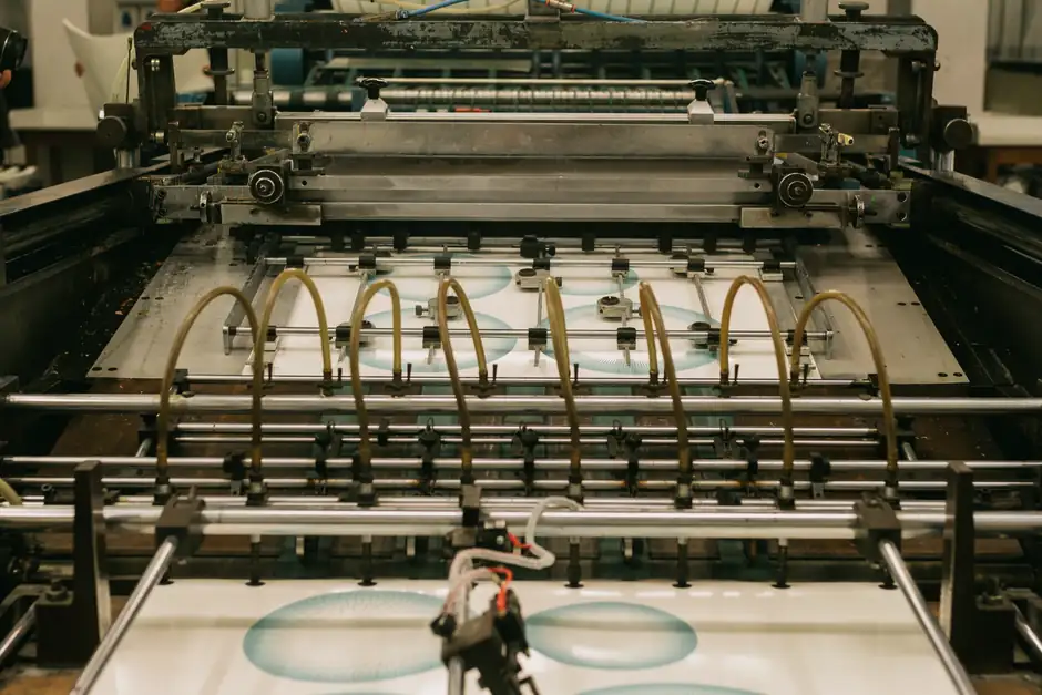
A spec-first buyer separates the substrate-making tool chain (crystal growth, wire saw slicing, lapping, etch, CMP) from the front-end chip-patterning tool chain (lithography, plasma etch, CVD/ALD, CMP, metrology), because the two share almost no hardware and mis-labelled RFQs draw quotes from the wrong half [S4][S7].
The combined wafer fab equipment (WFE) market is projected at USD 166.35 billion in 2025, growing to USD 344.36 billion by 2032 at an 11.0% CAGR, while the upstream wafer-manufacturing equipment segment alone sits at USD 18.6 billion in 2025, rising to USD 30.4 billion by 2035 at a 5.0% CAGR [S5][S8]. The two trajectories are driven by different forces: advanced-node patterning pulls the WFE number, while silicon substrate capacity and 300 mm transition pace the upstream number.
Where the Tool Chain Splits: Substrate vs Circuit Patterning
The wafer-manufacturing half runs crystal growth, cropping and OD grinding, wire-saw slicing, edge grinding, lapping, etching, polishing/CMP, cleaning, and metrology, with mainstream wafer sizes at 100, 150, 200, and 300 mm and a 300 mm nominal thickness of approximately 775 µm (200 mm: 725–775 µm) [S4][S7]. Standardization reference is SEMI M1 for polished single-crystal silicon wafers, with M1-0114 as the current family member cited in vendor literature [S4].
The front-end patterning half, by contrast, is dominated by lithography (EUV and High-NA EUV), plasma etch, CVD and ALD deposition, CMP, and in-line inspection and metrology; the top five vendors by share are Applied Materials, ASML, Lam Research, Tokyo Electron, and KLA [S5]. A university cleanroom program makes the same separation explicit, with substrate preparation (cut, ground, polished, cleaned) completed before any device layer is added [S4].
Wire-Saw Slicing: Kerf, TTV, and the Yield Ceiling
Wire-saw slicing is where most of the upstream yield loss originates: diamond-wire kerf loss runs approximately 70–150 µm per cut, compared to roughly 180–220 µm for legacy slurry multi-wire saws, and good-wafer total thickness variation (TTV) targets sit in the single-digit µm range as-sliced, with final flatness held to SEMI M1 [S4].
Subsurface damage from slicing propagates through every downstream step (lapping, etch, polish) and imposes what vendor guides describe as a hidden ceiling on yield for all processes that follow the wafer form factor, a number few suppliers disclose openly [S4]. Sourcing teams should ask vendors for in-process TTV and subsurface-damage data, not just nominal throughput. The economics of a wire saw line reduce to a single figure: cost per good wafer (CPGW), which folds kerf, breakage rate, and downstream rework into one comparable number across vendors [S4].
Wet-Bench Stations: Where Most Process Variability Actually Lives
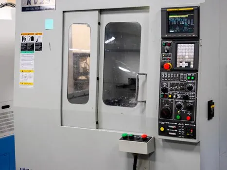
Wet processing, including acid and base (solvent) cleaning, development, and etch, is delivered across manual, semi-automated, and fully automated wet bench stations, with manual stations offering hands-on control at the cost of operator-dependent variability, semi-automated stations adding servo-controlled robotics for repeatable wafer etching and cleaning, and fully automated stations adding in-house designed robotics and software for tight control of process times, chemical dosages, and environmental conditions [S2].
Customization options on these benches typically include chemical management interfaces, specific construction materials (for HF, SC1, SC2 compatibility), data logging, and resistivity monitoring; vendors that design their own robotics and software in-house can iterate faster on a customer's specific chemical sequence than assemblers of off-the-shelf motion platforms [S2]. For new 300 mm lines, fully automated wet benches with closed-loop chemical dosing and resistivity monitoring are the default; manual benches are mostly retained for R&D and pilot lines.
Cleanroom, Tool Sub-Assemblies, and the Machining-Center Backbone
Semiconductor production equipment is operated in cleanrooms designed to minimize fine particles and contaminants, and each unit performs a specialized function while coordinating with the rest of the line to complete the production process [S3]. The workpieces that make up these tools, including frames, plates, showerheads, gas-delivery blocks, and chamber components, are themselves produced on high-rigidity machining centers capable of aluminum and stainless work at tight tolerances for the equipment OEMs [S3].
The relevance for industrial buyers is that wafer fab equipment is not just a single tool but a chain of sub-assemblies, each with its own supplier base, and the upstream machining and linear guide quality directly affects the downstream overlay accuracy and stage lifetime of the final tool. Sourcing teams that audit the sub-assembly supply chain, not just the OEM brand, catch the variability that determines mean time between failures on critical modules. Related motion-system engineering, such as crossed-roller guide selection for vacuum stages, is treated separately in the spec-first literature because the duty cycle and contamination budget differ from general industrial automation.
Patterning Half: EUV, High-NA EUV, and the Inspection Race
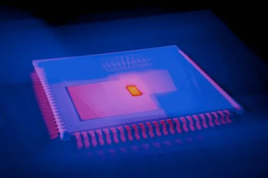
Converting 3 nm, 2 nm, and below roadmaps into production-ready chips requires fundamental step-changes in lithography (including EUV and High-NA EUV), deposition, etch, inspection, and metrology tools, and foundries and IDMs invest heavily in next-generation capital equipment to secure yield, throughput, and process control at these nodes [S5]. In February 2025, Applied Materials introduced the SEMVision H20 defect-review system, which merges cold field emission (CFE) electron-beam technology with AI-based image recognition, delivering up to 50% improved nanoscale imaging resolution, 10× faster imaging speed, and 3× higher throughput compared to legacy e-beam tools, targeting buried defects in 3D device architectures such as GAA transistors and 3D NAND/DRAM [S5].
For spec-first selection, the patterning half is dominated by the five top vendors (Applied Materials, ASML, Lam Research, Tokyo Electron, KLA), and the practical differentiators are resolution, throughput, and process node coverage rather than headline tool price [S5]. Buyers specifying new tools for sub-3 nm work should pin the RFQ to node, wafer size, and target defect density, not to a generic model code.
Selection Criteria and Comparison: Which Half Is For You
For a substrate house buyer, the required tool set is Czochralski or float-zone crystal pullers, wire saws, edge grinders, lapping and polishing tools, and metrology, with the dominant spec variables being wafer size (100/150/200/300 mm mainstream; 450 mm standardized but stalled), kerf loss (70–150 µm diamond wire), TTV (single-digit µm target as-sliced, SEMI M1 at finished polish), and CPGW [S4][S7]. For a circuit fab buyer, the required tool set is lithography scanners, plasma etchers, CVD/ALD deposition equipment, and CMP, with dominant spec variables being resolution, overlay, throughput, and defectivity at the target node [S5].
Buyers operating pilot or R&D lines that need both halves in a smaller footprint typically pull a manual or semi-automated wet bench for the substrate side and a used or refurbished scanner for the patterning side, and they accept lower throughput in exchange for capital flexibility [S2]. For a 300 mm production line, the two halves are almost never co-located: the substrate half goes to a silicon wafer plant, the patterning half goes to a fab, and the two connect only via wafer shipping. Related decisions on adjacent process infrastructure, such as NDT equipment selection for in-line defect review on chamber components, follow a separate spec-first framework and should not be conflated with the WFE RFQ.
Limitations, Failure Modes, and Sourcing Standards
The 450 mm wafer transition is standardized but stalled, so buyers planning beyond 300 mm should treat 450 mm capacity as speculative rather than proven [S4]. Slicing imposes a hidden yield ceiling from subsurface damage that propagates through lapping, etch, and polish, and few vendors disclose the subsurface-damage number on a datasheet, so RFQs should ask for it explicitly [S4].
Foundries and IDMs running advanced nodes face escalating capex per tool, with EUV and High-NA EUV systems carrying the largest single-line items and the longest lead times; the practical mitigation is multi-vendor sourcing of compatible sub-assemblies, not switching primary tool OEMs mid-node [S5]. For the substrate half, the reference standard is SEMI M1 (polished single-crystal silicon wafers), with the current M1-0114 family governing dimensional and flatness specs for 300 mm polished wafers [S4]. Buyers should also audit the upstream machining supply chain, including how OEM anti-static equipment and grounding logic on tool sub-assemblies is qualified, because ESD events during sub-assembly handling translate directly into field failures on the final tool.
What to Track Next
Two trackable signals for the next review window: (1) 300 mm polished-wafer capacity additions and the resulting CPGW movement, since the substrate half is growing at a 5.0% CAGR through 2035 and capacity tightness historically shows up here first [S8]; (2) High-NA EUV tool shipments from ASML and follow-on defect-review capacity from Applied Materials' SEMVision H20 platform, since the patterning half is growing at an 11.0% CAGR through 2032 and the bulk of incremental capex is concentrated at sub-3 nm nodes [S5].
See also our earlier report, Rebar Bender Maintenance for Landscaping and Hardscape Sites.