
Every modern NAND die is organised as an array of Blocks, each Block subdivided into Pages, and the page size has converged on either 2 KB + 64 B spare or the legacy 512 B + 16 B spare layout [S3]. A page is the smallest unit you can program or read; a block — typically containing 32, 64 or 128 pages on current planar/3D nodes — is the smallest unit you can erase, and that asymmetry is the single fact every downstream process (ECC strategy, wear levelling, bad-block management) has to accommodate [S3].
Inside each page, the Main Area holds user data (2,048×8 or 512×8 bits on x8 parts) and the Spare Area holds metadata (64×8 or 16×8 bits) used for bad-block flags and ECC parity [S3]. A representative Micron part cited in teardowns — MT29F2G08AxB — uses the 2 KB + 64 B geometry and reads/programs in page granularity [S3].
Page geometry, spare area and why x8 vs x16 matters
The two geometries still seen on incoming material are 528×8 / 264×16 bits per page for the older 512 B design and 2,112×8 / 1,056×16 bits per page for the current 2 KB design [S3]. A wider x16 interface doubles the I/O width but halves the addressable units per cycle, so controller and probe-card layout choices have to be locked before the wafer sort step [S3].
Spare area bytes are not user-addressable in the conventional sense; they are reserved for the factory bad-block marker and for runtime ECC (BCH, LDPC, or Reed-Solomon depending on node), and that split is fixed in the silicon — it cannot be repartitioned by the host [S3]. On a 2 KB page the ratio is roughly 64/2,112 ≈ 3 % spare overhead, a number process engineers use as a sanity check when reconciling raw die capacity against usable capacity on the spec sheet [S3].
Bad-block management: factory-marked vs grown
NAND flash is shipped from the fab with a known population of invalid blocks, called factory (masked) / initial bad blocks, and the manufacturer marks them in the spare area of the first or last page of each affected block [S2]. The contract is explicit: the stability of a marked bad block is not guaranteed — even a write that reports success may not be readable, and a read may silently corrupt — so the host controller is required to treat every flagged block as unusable from boot [S2].
Runtime block failures (grown bad blocks) are a separate category and only appear after programming/erase cycling; the controller's FTL or the kernel MTD layer is responsible for retiring them and remapping to a spare block pool [S2]. A 64 MiB Samsung part (Manufacturer ID 0xEC, Chip ID 0x76, 3.3 V x8) surfaced in an S3C2440 boot log demonstrates the conventional partition layout over a raw NAND device, with the MTD subsystem scanning for bad blocks and creating three partitions — "boot" at 0x00000000-0x00040000, a second region starting at 0x0004c000, and a third extending to 0x0024c000 [S1]. The offsets 0x00000000-0x00040000 and 0x0004c000 reflect the standard practice of skipping the first page of each boot block to avoid the bad-block marker byte, which is reserved for the BBT (Bad Block Table) when the partition is created [S1].
Program, read and erase timing on the host interface

The asynchronous NAND interface is governed by three timing parameters visible in the boot log: Tacls = 2 (≈ 20 ns), Twrph0 = 3 (≈ 30 ns) and Twrph1 = 2 (≈ 20 ns) on the S3C2440 SoC [S1]. These map directly to the command latch enable, write enable high, and write enable low strobes in the ONFI/JEDEC asynchronous timing diagrams, and they scale with the controller clock rather than with the NAND core — a frequent trap when porting a driver to a faster host [S1].
Because erase operates on an entire block while program operates on a single page, the worst-case write amplification from a single-byte host update is one full block-erase followed by one full block-program, and that asymmetry is the engineering reason ECC engines, wear-levelling tables and over-provisioned spare area all have to be sized together rather than independently [S3]. A practical reading of the 64 MiB 3.3 V x8 part gives 64 MiB / (2 KB + 64 B) = 31,744 pages, or 64 MiB / (16 KB + 512 B) = 4,096 pages per die depending on the assumed block geometry, and the order-of-magnitude check is enough to catch a misconfigured MTD partition table at bring-up [S1][S3].
Linux MTD layer: where the driver complexity actually lives
For a process engineer reading the Linux side of the stack, the headline from kernel bring-up work is that the hardware side of NAND is trivially simple — chip enable, command/address cycles, ready/busy polling — and the bulk of the code complexity sits in the MTD subsystem above it [S1]. The boot log line "S3C24XX NAND Driver, (c) 2004 Simtec Electronics" is the loading of the soc-nand.c glue, while "Creating 3 MTD partitions" and the subsequent "0x00000000-0x00040000 : 'boot'" entries are the generic MTD partition parser instantiating mtd_info structures that the UBI/UBIFS or jffs2 layer will later attach to [S1].
ECC placement within the spare area is the other place the MTD layer is opinionated: software BCH engines on small-page parts use 3-4 bytes per 512 B sector, 1-bit/4-bit/8-bit BCH variants use 7-13 bytes per 512 B sector, and on 2 KB-page parts LDPC engines can consume 30+ spare bytes per page, so the spare-area budget defined at the fab process step is consumed in one place, not distributed [S2][S3]. When ECC reports an uncorrectable error, the bad-block retirement path is triggered and the page is mapped out, which is why the initial scan phase of the driver has to walk the spare area of every block before any partition is mounted [S1][S2].
Comparison: x8 small-page vs x8 large-page vs x16 large-page
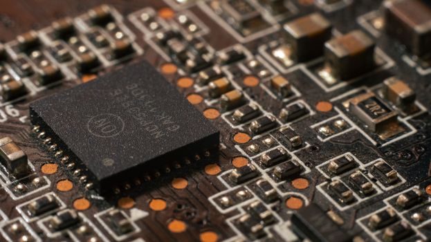
Three configurations still arrive in the field and the selection comes down to controller support, bandwidth and spare-area budget rather than raw capacity. A controller spec for the same die capacity will pick the x8 small-page (512 B + 16 B) variant when the host is a low-cost MCU without a 2 KB-internal-buffer DMA engine, the x8 large-page (2 KB + 64 B) variant when an SoC with an internal SRAM buffer and BCH hardware is in play, and the x16 large-page variant when the application is a high-throughput data logger that needs the wider bus to hit the throughput target without pushing the asynchronous interface above 50 MHz [S3].
On a criteria basis: spare overhead is 16/528 = 3.03 % for 512 B pages and 64/2,112 = 3.03 % for 2 KB pages, so the ratio is essentially the same across generations — the absolute spare area doubles, which is what enables stronger ECC and larger BBT entries on newer parts [S3]. Block-erase time on the order of 1-2 ms and page-program time on the order of 200-500 µs are the headline process limits that any write-throughput guarantee has to clear, and these have to be confirmed against the manufacturer's datasheet for the specific die revision because they move with process node, not with the [S3]-style page geometry assumption [S3].
Sourcing signals and where the spec sheets are authoritative
Manufacturer datasheets — Micron MT29F2G08AxB being a documented example — are the only source of truth for page size, block size, plane count, interface width, timing modes, endurance in P/E cycles and the initial bad-block marking convention, and the Linux MTD stack treats the values from ONFI parameter pages or the JEDEC legacy ID table as ground truth regardless of what the bootloader prints [S3]. The S3C2440 boot log captures the older JEDEC ID read path (Manufacturer ID 0xEC, Chip ID 0x76) rather than ONFI, so engineers porting to a modern controller should expect the parameter-page read command (0xEC) and the ONFI signature "ONFI" at offset 0x00 to be the first probe sequence on the bus [S1][S3].
Process engineers specifying NAND for a new design should treat the published JEDEC JESD230 (ONFI) timing modes and the manufacturer's qualified mode list as the binding constraints, and should not assume the asynchronous Tacls/Twrph0/Twrph1 numbers from a 2440-era driver are usable on a contemporary host [S1]. For comparison with adjacent process lines, the chip packaging smart manufacturing stack covers the back-end AOI/robotics handling that takes over once wafers are thinned and singulated, while battery cell manufacturing process 2026: electrode-to-formation spec stack is a useful analogue for reading NAND fab process maps because both industries organise their documentation around electrode-to-finished-cell and array-to-finished-die block/page hierarchies respectively. Two trackable signals for the next cycle: (1) the migration of the bad-block marker from the first/last page spare byte to a dedicated OTP region on 3D NAND generations, which would change the MTD scan loop, and (2) the consolidation of ONFI parameter-page reads with the toggle-mode DDR interface on newer Micron/Samsung/Kioxia parts, which would make the [S1]-style asynchronous ID read a legacy path on future controller bring-ups.
For component-level specifications, see additive manufacturing material, multifunction process calibrator, and v process line.