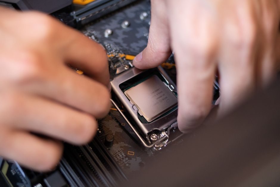
A modern CPU is the downstream sum of roughly 30 to 40 qualified input streams: a 300 mm silicon wafer, ~30+ photoresist layers, ultra-pure carrier and etch gases, an ABF organic substrate, a stacked HBM cache, and a basket of rare-earth and refractory metals for tool spares. Each stream carries its own purity class, lead-time band and dual-sourcing constraint, and the spec engineer treats every node as a separate line item on the BoM [S1][S2].
"Raw material" in this BoM sense means the input that still needs further processing before becoming a finished product — the same dictionary definition the chemical industry uses, whether the line in question is a cement kiln feed, a glass batch or a CPU wafer-start material [S3]. For a CPU program, that upstream chain now stretches across Taiwan, South Korea, Japan, the U.S. and the EU, with single-source exposure sitting on roughly half of the layers.
Silicon Wafer and Crystal Pulling: 300 mm, 200 mm and Wafer-Start Purity
The first gate is the wafer itself: a 300 mm mono-crystal silicon disc cut from a Czochralski-pulled ingot grown in a quartz crucible, with a defect-density band that has been falling node-on-node for two decades. Modern leading-edge CPU production is run on 300 mm wafers; trailing-edge and many automotive/industrial CPUs still run on 200 mm lines, and both formats have to be sourced as separate qualification streams. Wafer-start purity is normally quoted as parts-per-billion metallic contamination and a resistivity window in ohm-cm, both of which are part of the supplier datasheet rather than something a buyer can audit in-house. [S1]
Lead time on a 300 mm ingot is typically 8 to 14 weeks once a slot is secured with a primary vendor, and capacity is concentrated in five suppliers worldwide. For a buyer who needs a dual-source, the practical answer is a primary-plus-secondary allocation, not a true second-equivalent vendor — the second slot is almost always a trailing-edge spec or a smaller-diameter format. Pricing is quoted per wafer with separate adders for epi layers, SOI and ultra-thin back-grind, each of which moves the wafer from a commodity line to a custom-engineered input.
Photoresist, EUV-Resist and Patterning Chemistry
Resist is split into three families: g/i-line (mature nodes only), ArF immersion (the workhorse for current 7 nm-class CPUs) and EUV resist (the layer count grows node-on-node and is the single largest chemistry change since 2018). Purity classes run at sub-ppb metallic contamination and water content measured in ppb, with shelf life and temperature-controlled logistics treated as hard delivery conditions, not as a footnote. [S2]
Patterning chemistry is also where the under-layer, hardmask and developer streams attach. A typical ArF immersion resist ships with a matched bottom anti-reflective coating (BARC) and a tetramethylammonium-hydroxide (TMAH 2.38 %) developer, and each component has its own supplier chain. For EUV layers, the resist is co-developed with a specific spin coater track and a specific post-development bake recipe, so swapping the resist brand is rarely a drop-in change — it is a full re-qualification. The engineering cost of a resist swap at a mature node is commonly quoted as 8 to 12 weeks of wafer time on a monitor wafer before production wafers can be released, and that delay is what keeps most fabs on a primary resist vendor for any given layer.
Ultra-Pure Gases, Wet Chemicals and Ultra-Pure Water (UPW)

Etch and deposition tools consume specialty gases at purities normally quoted as 99.999 % to 99.9999 % ("5N" to "6N"), with the highest grades reserved for critical deposition steps. The active list includes NF₃, SF₆, CF₄, Cl₂, HBr for etch; SiH₄, Si₂H₆, H₂, N₂O, NH₃ for CVD/ALD; and a long tail of dopant and precursor gases. Each gas has its own delivery mode (bulk tube trailer, on-site generator, or cylinder), and a fab will typically run 10 to 20 different gas lines into a single tool. [S3]
Wet chemicals — SC1, SC2, HF, H₂O₂, IPA — and ultra-pure water (UPW, 18.2 MΩ·cm resistivity, TOC in single-digit ppb) are the second large chemistry block. UPW consumption at a leading-edge fab is commonly quoted at several million gallons per day for a single megafab. The supply side of these chemicals is more fragmented than the wafer side, which is what allows most fabs to keep two qualified vendors for any given chemical — but the same is not always true for the most aggressive HF and H₂O₂ grades, where the global supplier count is in the low single digits. A spec engineer evaluating a new fab site will audit gas and chemical bulk delivery as a hard requirement, not a soft cost line.
ABF Substrate, HBM Stack and Advanced Packaging Materials
The CPU no longer ends at the die. A modern high-performance CPU ships on an Ajinomoto Build-up Film (ABF) substrate, and the substrate is a single-source material on the leading edge — the global supply of advanced ABF is dominated by one Japanese vendor and a small group of Taiwanese makers, with new capacity still coming online. ABF layer count has been rising for several product generations, and the move to glass-core substrates is now a 2026–2027 watch item for spec engineers planning two product cycles out. [S4]
On top of the substrate sits the HBM cache, which is the densest memory stack in mass production. An HBM3E stack is a 12-Hi or 16-Hi TSV (through-silicon-via) DRAM pile on a base logic die, bonded with micro-bumps and an underfill, and assembled on an interposer or on a silicon bridge. The spec that matters at the CPU BoM level is the per-stack capacity (now 24 GB to 36 GB per stack) and the per-pin bandwidth (over 1 TB/s on HBM3E). For a full CPU socket, the HBM line item is one of the largest single non-wafer cost blocks — a fact the AI chip BoM 2026 article walks through at the system level. Advanced packaging also adds its own raw-material needs: copper-clad seed layers for plating, solder micro-bumps (often Sn-Ag-Cu or Sn-Ag), underfill epoxy, and the silicon interposer or bridge die itself, each of which is a separate dual-source decision.
Rare-Earth Elements, Refractory Metals and Tool Spares
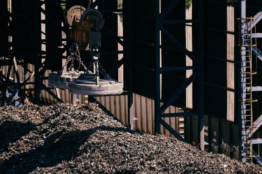
The chemistry is only half the input list. A leading-edge fab also burns through rare-earth and refractory metals as tool consumables: tantalum and tungsten for sputter targets and barrier layers, cobalt and ruthenium for liner and seed layers, hafnium and zirconium for high-k gate dielectrics, and rare-earth oxides such as lanthanum-oxide or cerium-oxide for specialty optical and polishing steps. Cobalt and ruthenium are the most exposed — both have small, concentrated supplier lists and 8 to 16 week lead times, and a fab will typically hold a 60- to 90-day safety stock for the most exposed lines. [S5]
CMP slurries, polishing pads and post-CMP cleaners are a parallel chemistry stream, with colloidal silica or ceria slurries, pad conditioners with diamond tips, and brush cleaners. Each of these streams has a dual-source option in most cases, but the dual-source partner is often a regional supplier rather than a global top-three vendor, and the qualification delta is non-zero. From a sourcing point of view, the rare-earth and refractory block is where the spec engineer spends the most time on geopolitical exposure — not because the volumes are huge, but because there is no fast replacement chemistry if a single source goes offline.
Power Delivery, Thermal Stack and the CPU Socket Bill
Outside the die, the CPU module bill includes a voltage-regulation stack (motherboard VRMs or, on高端 laptop and server SKUs, an on-package VR), a thermal interface material (TIM — indium, gallium-alloy or high-viscosity silicone), a heat-spreader (often nickel-plated copper), and the socket itself with its land-grid or pin-grid array. Each of these is a separate sourcing line with its own alloy spec and plating spec. Indium-based TIMs, for example, have a tight alloy window (typically In-Sn or In-Ag-Sn) and a single-digit °C/W conductivity target, and the linear guide reference is a useful reminder that a precision assembly on copper substrates is the same problem at a different scale: coefficient-of-thermal-expansion match, surface finish in nm, and a hard flatness spec. [S1]
The Intel-versus-AMD TDP comparison that the spec engineer sees at the desktop end is the downstream view of this whole material chain: a 125 W to 253 W desktop CPU running on a 200 mm or 300 mm die, on an ABF substrate, with a multi-phase VRM, an indium TIM, and a nickel-plated copper heat-spreader [S4]. The same CPU BIOS will then expose PL1/PL2 power limits, ring/cache ratios, and per-core multipliers that change the operating point second-by-second, so the material stack has to be qualified for the worst-case boost profile, not the steady-state TDP [S5].
Sourcing Levers, Dual-Source Strategy and Standards Watch
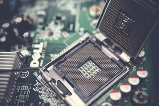
For a 2026 spec engineer, the practical sourcing checklist is short and unforgiving: a primary-plus-secondary wafer vendor with explicit allocation contracts; a single resist vendor per layer with a documented 8-to-12-week re-qualification plan for a backup; a gas and chemical list that hard-codes bulk delivery mode and 60-to-90-day safety stock; an ABF contract that is now typically a 12-to-24-month allocation, not a spot buy; an HBM capacity reservation tied to the CoWoS / advanced-packaging capacity of the foundry; and a rare-earth/refractory stock policy that is reviewed quarterly against the export-control list of the country of origin. The wider supply-chain context — how foundry capex, photoresist, EUV pellicle and OSAT capacity all knit together — is laid out in the semiconductor supply chain 2026 article. [S2]
The single most common failure mode is treating the CPU raw-material bill as a wafer problem. It is not. It is a 30-to-40-line bill where the wafer is the most expensive line but rarely the most fragile one — the most fragile lines are the EUV resist, the high-NA pellicle, the ABF substrate, the HBM stack, and the Co or Ru liner chemistry. The power transformer buying guide 2026 covers a different BoM, but the underlying sourcing logic is the same: the cheapest line is rarely the bottleneck, the bottleneck is the line with the fewest qualified vendors and the longest re-qualification window.
Next signal to track: ABF layer-count roadmaps and the first commercial glass-core substrate shipments, which are expected to migrate from sampling to low-volume production in 2026 and will re-rank the substrate line in any 2027 CPU BoM. Second signal: HBM4 capacity reservations at the CoWoS-S and CoWoS-L lines, which will set the upper bound on per-socket memory bandwidth through 2027.