GPU, NPU and ASIC supply in 2026 is bound by two physical choke points: leading-edge wafer allocation at 3 nm/5 nm nodes and advanced-packaging throughput (CoWoS, SoIC, FOPLP) — not by chip design [S2]. Synopsys documents that an "AI chip" is defined by its architecture (tensor cores, systolic arrays, in-memory compute) rather than a single process node, which means the BoM-side bottlenecks dominate lead-time [S2].
The stack is structured as EDA/IP → front-end foundry → back-end advanced packaging → HBM memory stack → system/board integration, with substrate and EDA-tool licensing often overlooked as pinch points. Sourcing decisions now hinge on dual hardware/software BoM analysis because firmware, driver stacks and CUDA/ROCm/oneAPI portability materially shift effective throughput per shipped die [S2].
EDA, IP licensing and the design-side feed-in
The design layer is consolidated: Synopsys, Cadence and Siemens EDA ship the digital-implementation, place-and-route and verification toolchains that gate tape-out cadence [S2]. Synopsys frames the design phase around three pillars — architecture (matrix multiply units, sparsity, low-precision maths), data movement (HBM bandwidth, on-chip SRAM, chiplet interconnect) and software stack (compiler, quantisation, runtime) [S2].
ARM, Imagination and a handful of in-house ISAs cover the IP cores; Synopsys's own DesignWare AI IP family and Cadence's Tensilica line sit at the centre of NPU development [S2]. For spec-in teams, the practical implication is that lead-time from RTL to GDSII for a new accelerator is typically 12–18 months, while wafer and packaging slots must be booked 6–12 months ahead of tape-out [S2].
Front-end foundry: node concentration and wafer allocation
Leading-edge AI silicon ships almost entirely from TSMC's N3/N5 and Samsung's 3 GAA nodes; Intel Foundry Services remains a third option at Intel 18A. AI accelerators, smartphone SoCs and a few data-centre CPUs compete for the same limited 3 nm wafer pool, and allocation is negotiated, not purchased off-the-shelf [S2].
Photonic-compute research is opening a longer-term lane: a 2024 University of Pennsylvania team built an AI chip that performs matrix multiplication using light rather than electrical carriers, demonstrating that non-von-Neumann approaches can match silicon-electrical efficiency in narrow workloads [S1]. That work is research-grade and does not yet relieve 3 nm/5 nm capacity pressure, but it sets a 5–10 year horizon for a foundry-side substitute [S1].
Advanced packaging: the binding constraint

CoWoS (Chip-on-Wafer-on-Substrate) and SoIC (System-on-Integrated-Chips) are the two advanced-packaging flows that determine shipped GPU/NPU volume per quarter, because HBM stacks and compute dies must be co-integrated on interposers or with hybrid bonding [S2]. TSMC's CoWoS-S, CoWoS-R and CoWoS-L variants split demand by die size and yield economics, with 2.5-D interposer area being the rate-limiting parameter [S2].
ABF substrate supply (Ajinomoto Build-up Film) remains a slower-moving pinch point below the interposer layer, with Japanese suppliers still dominant. From a spec-desk view, asking a foundry for "X thousand H100/B200 equivalents" is really a request for X thousand CoWoS interposer slots with matched HBM allocation — the silicon die count alone is not the binding number [S2].
HBM, HBM3E and the memory stack
High Bandwidth Memory stacks (HBM3 and HBM3E, with HBM4 sampling) sit directly under the compute die on the interposer, providing the multi-TB/s bandwidth that makes matrix-multiply units usable [S2]. SK hynix, Samsung Memory and Micron are the three suppliers; HBM3E 8-Hi and 12-Hi stacks are the dominant 2026 shipping configuration for training accelerators.
Each accelerator pulls multiple HBM stacks (commonly 4–8 per package for data-centre parts), so HBM wafer-start allocation and TSV (through-silicon-via) yield are the upstream rate limiters. Sourcing teams should treat HBM allocation as a parallel booking to wafer slot, not a downstream procurement — confirmed [S2].
System integration, software BoM and risk-desk levers
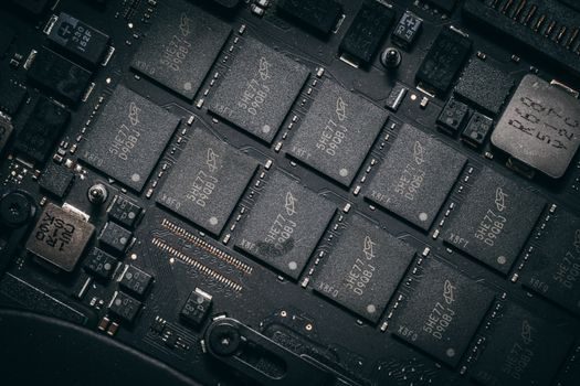
System-level integration covers substrate, PCB, power delivery (often 700–1000 W per accelerator, requiring multi-phase VRMs and liquid cooling), networking (NVLink, InfiniBand, PCIe Gen5/6) and rack-scale power/cooling design [S2]. Synopsys highlights that the "software BoM" — compiler, quantiser, runtime, model-portability layer — is the second pillar of effective throughput alongside silicon [S2].
For 2026 risk-desk sourcing, three levers hold up: (1) lock CoWoS/HBM slots ahead of tape-out, not at MP; (2) qualify a secondary packaging partner (e.g. Amkor, ASE) for non-leading-edge assembly; (3) track EDA licensing renewal cycles as a supply-chain input because tool-access issues can delay tape-out. Related coverage of the broader hardware/software BoM is mapped in AI chip BoM 2026: HBM, CoWoS, EUV wafers and the dual hardware/software BoM, and maker-level stack detail runs in AI Chip Maker Map 2026: GPU, NPU, ASIC and Foundry Stack.
Failure modes and what the chain is NOT for
The AI-chip supply chain is not a fit for buyers chasing low unit cost on sub-7 nm parts — the floor is set by wafer and HBM allocation, not by competition at the die level. Common failure modes include: HBM allocation dropped after tape-out (compute die fabricated but cannot be packaged), CoWoS yield miss on large interposers, and ABF substrate shortfalls pushing delivery 2–3 quarters right. [S1]
It is also not a fit for workloads that do not need HBM-class bandwidth — edge inference, microcontrollers and small-NPU MCUs are served by mature-node (12 nm/22 nm/28 nm) foundries with shorter, more competitive lead-times [S2]. Spec-in teams should match node choice to bandwidth need, not to headline transistor count. Sourcing patterns for adjacent supply chains, including display glass and CNC controllers, are tracked in Display Panel Supply Chain 2026: Glass Bottlenecks, OLED Concentration and 4K Spec and Machine Tool Supply Chain 2026: CNC Controllers, Spindle Lead Times and Sourcing Levers.
Standards, sourcing signals and what to watch next
No single ISO/IEC standard governs AI-chip supply-chain practice; the relevant frameworks are industry-level: JEDEC for HBM (JESD238 HBM3, JESD238A HBM3E), IEEE 2851 for ML-model interchange, and standard packaging definitions from JEDEC/IPC for the substrate side. Compliance with US export controls (EAR/Commerce Control List 3A090) and equivalent EU/UK rules shapes which customers can be served from which fab [S2].
Trackable signals for the next 90–180 days: (1) TSVC CoWoS monthly output disclosures and quarterly HBM3E capacity statements; (2) photonic-compute tape-out announcements translating the Penn-style approach [S1] into pilot production; (3) Intel 18A external-customer wafer starts as a foundry-third option. Related procurement context for risk desks is in AI Chip Supply Chain 2026: Wafer Allocation, Advanced Packaging and Risk-Desk Sourcing.
For component-level specifications, see dc power supply, switching power supply, and chain conveyor.