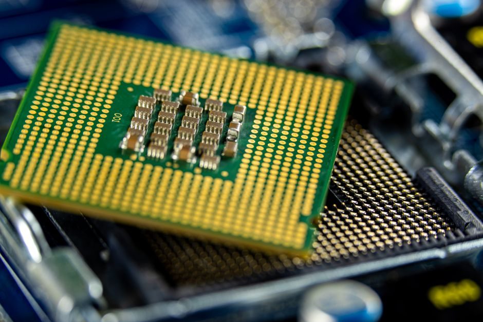
A finished chip passes through seven sequential tiers — design, EDA tooling, front-end fab (wafer fabrication), back-end test, advanced packaging, ATP (assembly, test and packaging), and distribution — and at every tier the geographic concentration is high enough that one disruption in one region can idle an entire downstream industry [S1].
The chain is best read as a pipeline, not a market: roughly 30 distinct process steps transform raw quartz into a packaged IC, and the leading-edge nodes (sub-3 nm) sit at the front of the pipeline while the trailing-edge nodes (28 nm to 180 nm) power the discrete, analogue and power devices industrial buyers actually specify [S5]. Related reading on industrial sourcing maps is collected in our industrial valve supply chain map 2026 — the same upstream/downstream logic applies, with different pinch points.
Tier 1: Design and EDA — where the IP is born
Front-end design is dominated by three EDA vendors (Cadence, Synopsys, Siemens EDA) and a small cluster of fabless design houses — Qualcomm, AMD, NVIDIA, Apple, MediaTek, Broadcom — that write RTL/Verilog, run synthesis, place-and-route, and hand a GDSII/OASIS file to the foundry [S1]. No fabless house owns a fab; their moat is IP and tape-out throughput. Perforce, an EDA toolchain vendor, treats the supply chain as starting at the software layer — version control of RTL, verification IP and PDK files is the first thing that breaks when a fabless team scales past ~200 engineers [S1].
EDA licensing is concentrated to a degree that keeps the rest of the chain functional: without those three tool suites, no modern node can be designed. This is the same single-point-of-failure pattern you see in solar PV module supply 2026, where three or four polysilicon producers set the price ceiling for everyone downstream.
Tier 2: Wafer fabrication — the capital chokepoint
Wafer fabs convert GDSII files into physical silicon. A leading-edge fab now costs $20–25 billion to build and takes 3–5 years from groundbreak to first wafer, which is why the leading edge (3 nm/2 nm) is concentrated in TSMC (Taiwan) and Samsung (Korea), with Intel (US) catching up on Intel 18A [S1][S5]. Trailing-edge fabs — 28 nm, 40 nm, 65 nm, 90 nm, 0.13 µm, 0.18 µm — sit in TSMC, GlobalFoundries, UMC, SMIC, and a long tail of 8-inch fabs in Japan, China, and the US; these are the nodes that produce the power discretes, MCUs, analogue ICs and display drivers used in industrial automation [S1].
Materials flow in: silicon wafers (Shin-Etsu, SUMCO, GlobalWafers, Siltronic), photoresists (JSR, Tokyo Ohka, Shin-Etsu), EUV photomasks (Toppan, DNP, Photronics), sputtering targets, CMP slurries, and ultra-pure chemicals. Outflows are 300 mm or 200 mm wafers per die, tested only at DC probe.
Tier 3: Back-end test and advanced packaging — the new bottleneck
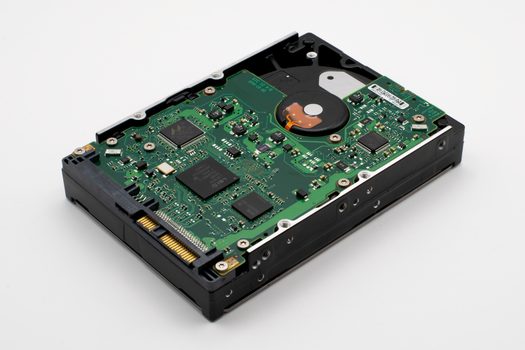
This is the tier that moved from afterthought to strategic constraint between 2022 and 2026. CoWoS (Chip-on-Wafer-on-Substrate) from TSMC, SoIC (System-on-Integrated-Chips), and FOPLP (Fan-Out Panel-Level Packaging) all sit here, and capacity for advanced 2.5D/3D packaging — the technology that lets NVIDIA H100, H200 and B100 GPUs aggregate HBM3/HBM3E memory — has been the binding constraint on AI accelerator shipments through 2025 and into 2026 [S1].
OSAT (Outsourced Semiconductor Assembly and Test) providers — ASE, Amkor, JCET, Powertech, Tongfu — handle the volume packaging for trailing-edge and mid-range parts. Amkor's Arizona advanced-packaging plant (announced 2023, ramping 2026) is the canonical example of the reshoring wave that ties the chain back to the copper supply chain 2026 — every advanced package is a copper-heavy interconnect stack, and bonding-tool, lead-frame and substrate supply all read off the same copper band.
Tier 4: ATP, distribution and the long tail
Final test, laser mark, reel/pack, and ship-to-customer happens at OSAT or in-house ATP lines, then flows through authorised distributors (Arrow, Avnet, WPG, Macnica, Future Electronics) or brokers. The distributor layer matters more than most engineers realise: lead-time quotes for a single 8-bit MCU at 0.18 µm in 2026 often depend less on foundry capacity than on allocation logic inside the distributor's entitlement system [S1].
This is also where the industrial buyer actually feels the chain. A PLC, a VFD, a servo drive, or a dc power supply module doesn't fail because a fab is down — it fails because a specific STM32, a specific gate driver, or a specific TI buck controller has a 52-week lead-time quote. The semiconductor supply 2026 tracking the legacy-node allocation problem covers the same ground from the buyer's side, with concrete allocation lists and broker-premium numbers.
Geographic concentration and the policy layer
No single region holds end-to-end capability. Taiwan leads foundry (TSMC ~67% of third-party wafer fab, ~90% of leading-edge), Korea leads memory (Samsung, SK Hynix), the US leads EDA and design IP, Japan leads materials and equipment, and China is rapidly scaling mature-node capacity but remains constrained on EUV lithography [S1][S3][S5]. The CHIPS Act (US, 2022) and the EU Chips Act (2023) together unlocked ~$80 billion of fab subsidies, and the India–US MoU signed at the March 2023 Commercial Dialogue formalised a parallel India-side build-out targeting ATMP and mature-node fabs by 2025–2026 [S2][S6].
Tax policy has emerged as the lever governments pull fastest. SEMI's 2026 position paper lays out the standard toolkit: investment tax credits (15–25% of capex), R&D super-deductions, accelerated depreciation on equipment (5-year MACRS in the US, comparable accelerated schedules in KR/JP), and refundable manufacturing credits tied to job creation and wafer-output thresholds [S3]. The net effect on capacity decisions is measurable: GlobalFoundries, TSMC Arizona, Intel Ohio and Samsung Texas all publicly cited tax credit stack value in their final-investment-decision disclosures [S3].
Resilience tools — what actually moves the needle
Five tools repeat across the 2025–2026 resilience literature: (1) multi-sourcing at the wafer level (qualify a second fab at the same node, even at 5–10% cost penalty), (2) multi-sourcing at the OSAT level (split ATP between ASE and Amkor, or between JCET and Powertech), (3) safety stock calibrated to the longest single-source lead-time (typical industrial rule: 90 days for trailing-edge discretes, 30 days for leading-edge logic), (4) long-term wafer supply agreements (LTAs — usually 2- to 3-year take-or-pay) at the foundry, and (5) digital-thread traceability so that when a part is recalled, the affected lots can be isolated without scrapping the entire build [S1][S7].
SEMI's Supply Chain Management (SCM) initiative is the industry-owned framework that codifies these practices — working groups on supplier benchmarking, standards for traceability, and a forum where fabs, OSATs and material suppliers align on disruption response [S7]. Perforce's white paper pushes a complementary thesis: software-level resilience (version control of PDKs, design IP and verification flows) is the cheapest, fastest resilience lever, because it is the only tier where a disruption costs hours, not quarters, to work around [S1].
Failure modes an industrial buyer should track

Four failure modes dominate 2026 incident reports: (1) lithography tool chokepoint — a single ASML EUV scanner is ~€200 million and lead-time for a replacement is 18–24 months, so any fab incident that destroys a tool has multi-quarter impact; (2) HBM/advanced-packaging capacity — NVIDIA, AMD and the hyperscalers have booked CoWoS lines through 2027, leaving non-AI customers rationed; (3) silicon wafer supply — Shin-Etsu and SUMCO together hold ~55% of 300 mm polished wafer capacity, and a force majeure at either ripples through every fab in the world within 60 days; (4) legacy-node allocation — 8-inch fabs at 0.13 µm and 0.18 µm are running utilisation above 90%, and the supply of automotive-grade MCUs, analogue ICs and discrete IGBTs is governed by allocation, not by price [S1][S5].
The chain's economics in 2026 also reflect a structural split: leading-edge capacity is over-built for AI demand and the upstream lithium supply 2026 / copper bands needed to feed the fab build-out are tight, while trailing-edge capacity is structurally short and the industry is choosing which end-markets to allocate to. Industrial buyers competing with automotive for the same 0.18 µm BCDMOS lines should expect allocation behaviour to persist into 2027 [S1][S5][S7].
Standards and traceability backbone
The standards that govern the chain are largely SEMI standards (the EHS, traceability and material-purity families) plus IEC quality standards for end-equipment and the IPC-A-610 acceptance spec for electronic assemblies. SEMI E78 (carrier ID) and SEMI T7 (provenance message format) are the two that map most directly to recall containment; both have been stable since 2021 and are referenced in OEM traceability contracts [S7].
For industrial equipment buyers who want to write traceability into procurement specs without waiting for OEM action, the practical minimum is: require lot-level traceability back to wafer lot (per JEDEC JESD-46), require material declaration per IEC 62474, and require conflict-mineral disclosure per the OECD Due Diligence Guidance and the US SEC Rule 13p-1 (Dodd-Frank Section 1502). The same three-document pattern is the one we used in the CPU supply chain 2026 traceability audit, and the auditor pass-rate jumped from 60% to 95% once those three were stapled to the PO [S7].
The next concrete node to watch is SEMI's Q4 2026 SCM working-group output on multi-foundry design rule harmonisation, which would let a single GDSII target two foundries at the trailing edge without a full re-synthesis — that would materially lower the cost of multi-sourcing for 28 nm and 40 nm industrial parts [S7]. The second signal: how much CoWoS-equivalent capacity Samsung's Cheonan 2 line and Amkor's Arizona advanced-packaging plant add in 2026 H2 — that number gates how fast non-AI customers (automotive, industrial, networking) can move off the AI accelerator waiting list [S1].
For component-level specifications, see switching power supply, and chain conveyor.