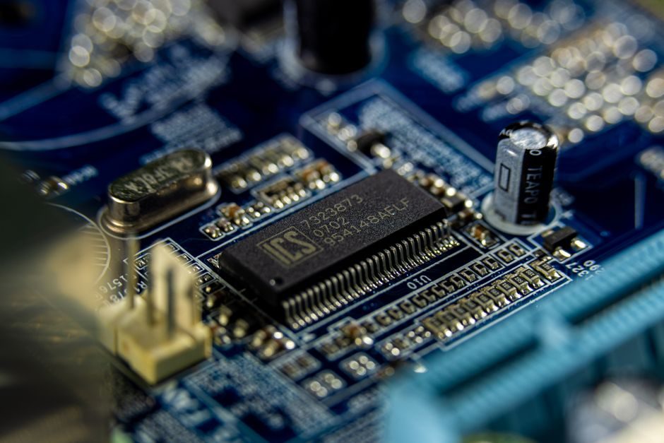
An AI accelerator's bill of materials now runs on two parallel ledgers: a hardware BoM dominated by HBM stacks, CoWoS interposer capacity, EUV-class silicon wafers and high-end ABF substrates, and a software/AI BoM that tracks firmware, BSP layers, model checkpoints and the agent/API surface that the silicon is actually asked to run.
The procurement question is no longer "what is on the PCB" but "what is on the die, in the package, and in the runtime stack", and a December 2024 export-control action by China on gallium, germanium, antimony and other key chipmaking minerals is still shaping how that hardware ledger is being hedged in 2026 [S5].
Hardware BoM: the four line items that drive AI accelerator cost
[S1]
The advanced-packaging step that glues those parts together — CoWoS-S or CoWoS-L with silicon interposers, or emerging panel-level fan-out — sits at the top of the queue constraint, and capacity at the leading OSATs is still being rationed wafer-by-wafer; the substrate underneath is an ABF (Ajinomoto Build-up Film) laminate, whose supplier base is concentrated in Japan and Taiwan and is now treated as a strategic sub-line on most OEM BoMs.
Materials flagged by the December 2024 China export-control list — gallium (GaN/GaAs RF and power), germanium (SiGe channels, some optical), antimony (advanced phase-change and infrared compounds) and several rare-earth families — sit several layers down the BoM but still surface in RF front-ends, power-delivery magnetics, photodetectors and some advanced packaging steps, which is why a sourcing desk that previously ignored the periodic table now keeps a separate critical-minerals sheet [S5]. For the upstream wafer-allocation picture, see this year's supply-chain read on wafer allocation and advanced packaging.
Where HBM, CoWoS and EUV actually pinch
HBM stacks are not interchangeable commodities: HBM3E is in volume production with 8-Hi and 12-Hi stacks on a 16 Gb–24 Gb per-die density, while HBM4 samples are shipping in limited windows to early-access AI customers; the practical ceiling per stack is the 1024-bit interface running at multi-Gb/s/pin, and the BoM line item is typically quoted per-GB rather than per-die, which is why an accelerator moving from 80 GB to 192 GB of HBM can move the package price by tens of percent. [S2]
CoWoS capacity is the harder constraint: silicon interposers are limited by reticle size (roughly 830 mm² in the current generation, with mask-stitching pushing the practical upper bound higher), and the OSATs running CoWoS-S/L have publicly guided that effective wafer-equivalent output is still rationed through 2026, which is why some hyperscalers are taking direct capacity reservations rather than buying packaged parts on the open market. The CoWoS/HBM interaction is covered in more depth in the GPU supply-chain write-up on CoWoS and HBM bottlenecks.
EUV wafer throughput is the floor under the whole stack: an EUV-layer-heavy AI die needs ASML NXE:3800E-class tools running at 150–180 wafers-per-hour production rates, and each layer adds dose/budget pressure; the practical fallout is that the leading node is effectively supply-limited even before the HBM and CoWoS lines are added, which is why a single accelerator BoM can be hedged with three different wafer-foundry options or with capacity reservations at the foundry level rather than at the packaged-part level.
Software BoM and AI BoM: the ledger above the silicon
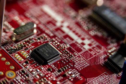
For SoC and system design, the "software" line item is no longer just the application: Perforce's 2026-01 guidance on compliant software BoMs for SoC and system design treats firmware, bootloaders, microcode, drivers and Board Support Packages (BSPs) as first-class parts of a delivered product, with the SBOM carried through to comply with NTIA-aligned minimum fields (supplier, component name, version, dependencies, author of SBOM data, timestamp) and to support vulnerability lookups against CVE/NVD feeds [S1].
A separate but parallel ledger — the "AI BoM" — has emerged to track the model and agent surface that the silicon is asked to run: the open-source ai-bom project on GitHub describes its purpose as letting an operator "discover every AI agent, model, and API in your infrastructure", with the project logging 279 commits at the time of the snapshot and a demo-project reference implementation [S2]. Practically, that means procurement teams are now expected to inventory, per accelerator deployment, the LLM checkpoints, embedding models, retrieval indexes, agent frameworks, and the API endpoints the agents call, with a unique identifier and a version pin for each.
The two ledgers meet at the runtime: the SBOM tells you what the silicon will execute from cold-boot, and the AI BoM tells you which model weights and agent policies are loaded; for a 2026 AI deployment, the audit-ready artefact is a signed SBOM for the firmware/BSP stack plus a versioned AI BoM for the model/agent inventory, both kept under change control.
Comparison: hardware BoM tiers and the matching software-BoM discipline
Across today's AI-accelerator programmes, the procurement picture splits into three working tiers; the table below lines them up against the criteria a sourcing desk is actually asked to defend. [S3]
Tier 1 — frontier accelerators (single-die 3 nm/N3P or 2 nm-class logic + 4–8 HBM3E/HBM4 stacks on CoWoS-S/L): highest per-package BoM cost, dominated by HBM and CoWoS; software BoM must track signed firmware, signed BSP, signed model weights, and a versioned AI BoM for every deployed agent; supply risk concentrated at HBM supplier, OSAT CoWoS line, and the EUV-stepping foundry.
Tier 2 — mid-range training/inference (5 nm/N4P-class logic + 2–4 HBM3 stacks, often CoWoS-R or 2.5-D fan-out): HBM is still the single biggest line item but with lower GB-count and lower per-GB cost; software BoM is materially the same shape (signed firmware + BSP + AI BoM) but with fewer agent frameworks in the inventory; supply risk is more balanced between foundry and OSAT.
Tier 3 — edge/inference accelerators (7 nm–12 nm logic, LPDDR5/LPDDR5X instead of HBM, often no advanced packaging): silicon and PCB BoM dominate over memory and packaging, but the AI BoM still has to be present, especially if the edge device runs a quantised model with periodic OTA weight updates; the firmware/BSP side of the SBOM often matters more here than at the data-centre tier because the device is physically exposed.
Sub-line items that quietly move the BoM: substrates, masks, gas and minerals
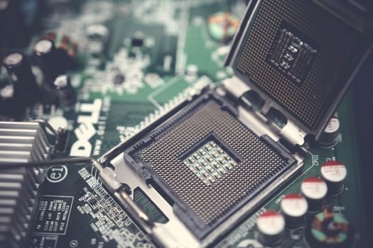
ABF substrates (resin-coated copper build-up films, dominated by Ajinomoto and a handful of Taiwanese/Japanese laminate vendors) set the practical maximum reticle-equivalent area that a CoWoS interposer can sit on, and a 2026 substrate shortage is a recurring theme in OEM earnings calls; lead times on the largest-area ABF panels still run into multiple quarters, which is why the substrate line is being treated as a strategic sub-line on AI-accelerator BoMs rather than a commodity. [S4]
EUV pellicles, photomasks and EUV-grade gases (neon, krypton, xenon mixes, fluorine precursors) sit one layer further down but still drive yield; the relevant sourcing note from December 2024 is that China restricted exports of gallium, germanium, antimony and "other key minerals" to the US, and these elements feed RF front-ends, SiGe channels, certain advanced packaging alloys and several compound-semiconductor optoelectronic lines, so a procurement BoM that previously listed "misc. materials" now has to name these specifically and qualify a non-China source [S5].
Rare-earth-driven materials also feed upstream of the BoM: the South China University of Materials Science and Engineering lists organic optoelectronic materials, inorganic non-metallic materials, polymeric and composite materials, metallic and surface engineering materials, and functional/energy materials as its five research thrusts — a useful taxonomy for a sourcing desk that needs to map a "material grade" in a BoM back to a research cluster and a credible supplier pool [S3].
Failure modes, constraints and audit signals
The two BoM layers fail in different ways, and the procurement risk picture has to cover both: a hardware BoM failure shows up as an HBM vendor change, a CoWoS interposer yield miss, a wafer-stepper throughput dip, an ABF substrate lead-time slip, or a critical-mineral export-control action — each of which can move the package price by double-digit percent in a quarter, as the December 2024 China action on gallium/germanium/antimony demonstrated when it rippled into 2025–2026 sourcing contracts [S5].
A software/AI BoM failure shows up differently: a signed firmware image that fails secure-boot verification, a BSP that drops a driver for a PCIe switch, a model checkpoint that is replaced without re-evaluating the agent policy on top of it, or an AI BoM inventory that lists an API endpoint which has since been deprecated; in all of these cases the silicon is fine but the delivered system is no longer the one that was qualified, and the audit trail is the AI BoM, not the silicon BoM [S1][S2].
Trackable signals for 2026-07 onward: (a) any change in the US/EU/Japan critical-minerals tariff or export-control list beyond the December 2024 baseline, (b) HBM4 volume-ramp announcements from the three major HBM suppliers against the CoWoS capacity reservations already booked, (c) ABF substrate capacity additions and lead-time trends, and (d) convergence of the SBOM and AI BoM standards — whether the AI BoM ends up as a separate artefact, an extension of the SBOM, or an upstream input to it.
For component-level specifications, see shaft key, pressure transmitter, and flow meter.