
The flat-panel display (FPD) manufacturing process is a multi-stage, cleanroom-controlled flow that turns glass substrates into finished LCD, OLED, and micro-LED panels through array fabrication, cell assembly, and module integration [S2].
Three Technology Branches Share One Substrate Flow
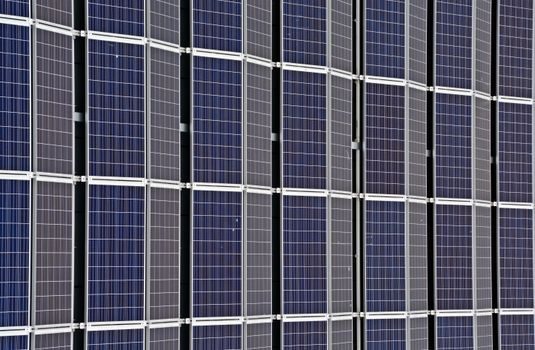
a-Si TFT, LTPS, IGZO, OLED evaporation, and micro-LED mass-transfer all originate on a glass substrate (Gen 4.5 730×920 mm through Gen 10.5 2850×3050 mm) processed inside a Class 100–1000 cleanroom [S2].
The four-phase process — substrate cleaning, TFT array formation, color filter / OLED stack, and cell assembly — is identical in topology for LCD, OLED, and micro-LED; the differences live in which deposition, patterning, and bonding tool set populates each phase [S2]. For a deeper look at how AI vision now gates the same kind of phase-by-phase inspection, see this PV smart-manufacturing breakdown of 2026 spec gates. LCD dominates unit volume on Gen 8.5/10.5 lines; OLED is built on LTPS backplanes with FMM evaporation; micro-LED adds a separate mass-transfer step with transfer yields typically well below 99.9% at the wafer-to-backplane handoff.
Array Phase: Deposition, Lithography, Etch, and Anneal
The TFT array is fabricated by repeating four sub-steps — conductor/insulator deposition (sputter or PECVD), photolithography (typically 4–8 mask layers for a-Si, 9–12 for LTPS), wet or dry etching, and dopant/activation anneal — across the full mother-glass area [S2].
Channel material defines the electrical spec: a-Si TFT hits electron mobility around 0.5–1 cm²/V·s, LTPS poly-Si reaches 50–100 cm²/V·s, and IGZO sits between at 10–30 cm²/V·s, which is why IGZO is the backplane of choice for high-resolution 8K LCD and large-area OLED [S2]. Critical-dimension (CD) tolerance on the TFT channel is typically held to ±0.5 µm, with overlay error between mask layers specified below 1.5 µm on Gen 6 substrates and tighter on larger Gen 8.5/10.5 lines. Inline metrology — ellipsometers for film thickness, four-point probes for sheet resistance, and AOI for defect density — sits between every mask step because rework is not possible once the next layer is deposited.
Cell Phase: Alignment, Seal, ODF/Filling, and Encapsulation
ODF volumes of LC material are controlled to ±0.1 mg per panel, and cell-gap uniformity is held inside ±0.2 µm across a Gen 8.5 substrate to keep retardation and contrast inside spec [S2]. For OLED, the encapsulation stack — typically a stack of inorganic Al₂O₃ or SiNx over organic acrylate — must push water-vapor transmission rate (WVTR) below 10⁻⁶ g/m²·day to keep cathode oxidation and dark-spot growth inside warranty. Spacer density and post-seal anneal profile are the two single biggest levers on cell-gap uniformity; a 1 µm shift in cell gap moves a normally-black VA-mode panel's contrast by roughly an order of magnitude.
Module Phase: Scribing, Bonding, Driver-IC Attach, and Optical Lamination
Module integration begins with mother-glass scribing — wheel or laser scribe + break for LCD, laser-only for flexible OLED — then COG (chip-on-glass) or FOG (film-on-glass) bonding of the source driver, COF bonding of the gate driver, and finished-panel lamination with polarizer, retardation film, and cover glass [S2].
COG bonding pitch sits at 20–35 µm with bonding force controlled inside ±0.5 N per IC bump to keep ACF (anisotropic conductive film) joint resistance below ~50 mΩ per bump; laser lift-off for flexible OLED runs at 308 nm excimer wavelengths at fluence controlled to ~200 mJ/cm² to release the polyimide from the carrier glass without damaging the TFT stack [S2]. Optical lamination adds an OCA (optical-clear-adhesive) layer between cover glass and panel; refractive index matching inside ±0.005 and bubble-free lamination are the visible-quality gates — a single 50 µm bubble in a 65" panel is a reject. Process control here shares the same MES-driven inspection logic used in battery cell stacking, as discussed in this [lithium-battery smart-manufacturing piece on cell-to-pack automation and AI inspection](/news/lithium-battery-smart-manufacturing-2026-cell-to-pack-automation-ai-inspection-and.html).
Process Options Side-by-Side: a-Si/LCD vs LTPS-OLED vs Micro-LED
Three competing display-panel options line up against four spec-driven criteria: a-Si/LCD is the cost baseline at ~0.5–1 cm²/V·s mobility and ≥85% NTSC color gamut via white-OLED + QD film; LTPS-OLED hits 50–100 cm²/V·s mobility, >100% NTSC, but at 2–4× the panel cost and yield losses of 10–30% during FMM evaporation; micro-LED pushes to >120% Rec.2020 and intrinsically long lifetime, but mass-transfer yields and defect-repair economics still keep unit cost above OLED for the foreseeable 2026 horizon [S2].
Selection matrix — for ≥75" TVs: a-Si LCD or IGZO LCD; for premium smartphone/IT: LTPO-OLED; for AR/μ-display and niche signage: micro-LED or OLED-on-silicon [S2]. Glass-substrate thickness dropped from 0.7 mm (Gen 8.5) to 0.5 mm then 0.4 mm to reduce weight, and flexible OLED now runs on 30–50 µm polyimide carriers. The dominant 2026 spec gate at panel-level is Mura (luminance non-uniformity) under 1.5% — that number is the single biggest predictor of finished-display yield across all three technologies.
Process Limitations and Failure Modes
Particle adders above 0.3 µm density the cleanroom out of Class 1000 and cause >90% of array-line yield loss; ODF over-fill pushes the cell gap down and triggers Mura, under-fill pulls it up and triggers image-sticking [S2].
Laser lift-off thermal budget is the hard ceiling on flexible OLED throughput — push the fluence and the PI carrier delaminates cleanly but the TFT stack sees peak temperatures above 350 °C that crack oxide semiconductors; pull it back and residual adhesion drops yield at the next step. LTPS excimer-laser anneal (ELA) carries a similar trade-off: full-melt crystallization gives the best mobility but the worst surface roughness, and partial-melt mode is the working compromise on Gen 6 lines. Micro-LED mass-transfer tolerance is currently the binding constraint on the entire process — even at 99.99% transfer yield, a 4K panel needs near-zero missing-pixel repair to be saleable, and the rework loop (selective pick-and-place + photoluminescence repair) is the single largest capex line in any new micro-LED fab.
Process Control and Standardized Spec Gates
HORIBA and similar metrology suppliers position in-line chemical-analysis and control equipment (liquid-particle counters, gas-impurity analyzers, endpoint detectors for plasma etch) as the spec-gate enablers across the entire FPD flow [S2].
Inline film-thickness measurement at 1 nm repeatability, sheet-resistance mapping at 0.1% precision, and residual-gas monitoring for moisture below -80 °C dewpoint are the three metrology specs that fabs quote on datasheets [S2]. Process control here overlaps with the same MES/IIoT stack used in heavy-industry smart manufacturing; the wiring of analyzers, recipes, and SPC charts onto a single platform is described in this natural-gas smart-manufacturing MES/IIoT piece. The controlling engineering concept is SPC-driven Mura control: a single CAPA cycle on one etch bath can shift 0.1 µm in CD and a downstream luminance delta of 0.3% — small numbers, but above 1.5% Mura, finished TV panels get sorted down to monitor SKUs or scrap.
Who This Process Is For (and Who It Is Not)
The FPD process flow is for: panel makers scaling a-Si LCD on Gen 8.5/10.5 for TV and monitor SKUs; OLED fabs running LTPS or LTPO on Gen 6 flexible lines for smartphone/IT; micro-LED pilots for AR micro-displays and large-format signage [S2].
It is NOT for: passive-matrix character LCDs (different supply chain entirely), e-paper (electrophoretic frontplane, no TFT backplane), and DLP/LCoS micro-displays (single-chip, not flat-panel). Fab newcomers without Class 100 cleanrooms, 4–8 mask lithography capability, and 200–400 °C thermal budget on PI-friendly tooling should not attempt this flow; the capex floor for a Gen 6 OLED line is well above USD 4 billion.
Trackable signals for the next quarter: (1) Gen 8.5 IGZO line ramp announcements and the first 0.4 mm-thick 65" panels shipping in volume, and (2) micro-LED mass-transfer equipment moving from sub-99.99% to 99.99%+ demonstrated yield at conferences — the second is the single best leading indicator that micro-LED panel cost will cross the OLED ceiling in 2027–2028.
For component-level specifications, see industrial display, additive manufacturing material, and multifunction process calibrator.