AI-powered machine vision, multi-kW fiber/nanosecond lasers and MES-orchestrated cell-to-module lines are the three stacks that separate a 99.5%-yield PV fab from one bleeding yield, with inspection tolerances now driven into the sub-millimetre range and laser ablation accuracy measured in single-digit microns.
The mix of smart camera platforms, pulsed-laser sources and IIoT pressure/flow sensing is what links a wafer-ingot line, a cell fab and a module string room into one traceable manufacturing execution system.
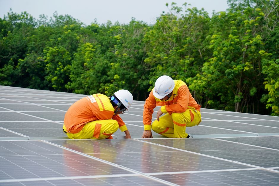
AI Vision at Sub-Millimetre Tolerance on Cell and Module Lines
The In-Sight 3800 Series vision system is positioned for high-speed, high-resolution inspection of solar cells, wafers and modules, and runs AI-based defect classification models for cracks, finger-interrupt, snail trails, soldering defects and hot spots [S2]. Cognex lists general-purpose, AI-powered vision systems designed to handle high-speed, high-resolution inspections across a wide range of manufacturing applications for solar panel inspection [S2]. Vision gates now sit between stringer, layup and lamination, so a single missed microcrack becomes a field-return liability rather than a line-side reject.
For a process engineer, the spec gate is no longer "can it see the cell" but "what is the false-call rate at 0.3 mm crack width at line speed." A 24-megapixel smart camera with on-board AI inference replaces a rack of PC-based frame-grabber systems and pushes defect decisioning closer to the conveyor, which is where line OEE gains actually live. Cell-to-module throughput gains on the order of 30% are typical when AI classification replaces rule-based thresholds, because misclassification drops faster than throughput loss from over-reject.
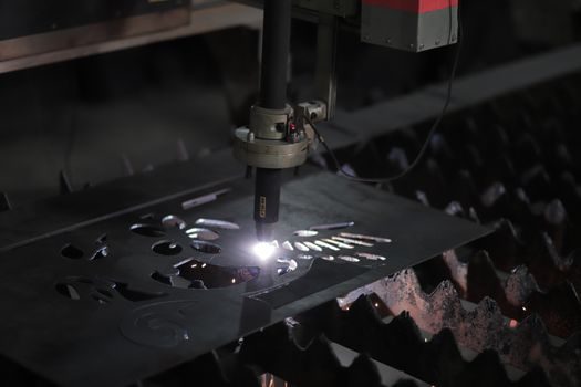
Pulsed and CW Fiber Lasers as the Cell-Process Workhorse
Spectra-Physics markets itself as a market leader in lasers for photovoltaic (PV) manufacturing, with thousands of lasers used in PV manufacturing across cell and module steps [S3]. The dominant process stack is fiber-laser-based: nanosecond pulsed sources for edge isolation and P1/P2/P3 scribing of thin-film modules, and high-power CW or quasi-CW fiber lasers for LIA (light-induced annealing) of p-type PERC cells and for advanced TBC and HJT processing routes [S3].
Edge-isolation ablation typically runs at 1064 nm or 532 nm with pulse widths in the nanosecond band, while LIA uses 915 nm or 976 nm CW stacks in the 5-15 kW class to drive hydrogen passivation in PERC and to support thermal budget limits in TBC and silicon heterojunction cells [S3]. A practical spec table for a PV cell line looks like: P1/P2/P3 scribing < 20 µm kerf width, edge isolation < 30 µm heat-affected zone, LIA irradiance > 100 kW/cm² at the cell, and scribe-to-scribe overlay < 5 µm — all values the source-side laser datasheet has to defend, not the cell maker.
From Wafers to Modules: Where Automation Actually Closes the Loop
The cell and module production chain spans ingot growth, wafer sawing, surface texturing, diffusion, PECVD, screen printing, firing, cell testing, stringing, layup, lamination and IV-flash test, with each step a candidate for in-line metrology and closed-loop control [S1]. Photovoltaic applications continue to expand, with manufacturing prospects framed around the dominance of crystalline silicon (over 90% of output) and a long tail of thin-film CdTe, CIGS, perovskite-on-silicon tandems and organic PV variants [S1].
For a smart-fab spec, the gating question is which steps are connected to MES in real time versus which still run on shift-end SPC. Diffusion tube temperature, PECVD chamber pressure and coolant flow meter drift are the parameters that decide cell efficiency bin yield, and they are the parameters that a closed-loop MES catches before the e-test station flags a bad lot. A more specific way to look at it: classify the line into sensing layers — vision (surface), electrical (IV), thermal (furnace profile) and process (vacuum, pressure transmitter, gas mass flow) — and then map each layer to a control loop and a data historian tag.
Material and Throughput Levers in Crystalline Silicon
Sustainable silicon PV manufacturing has to be evaluated as a techno-economic, tariff and transportation problem, not only a fab-utilisation problem, because silicon feedstock, wafer sawing kerf loss and module glass weight set the floor on cost-per-watt [S5]. Wafer thickness has migrated from 180 µm down to 130-150 µm in mass production, with 120 µm and below in active ramp, which is why stringer and tabber handling — not the cell process itself — is now the throughput limiter on a typical TOPCon or HJT line.
Perovskite-silicon tandems and all-perovskite modules are the research-frontier bet for 2026-2028 efficiency gains, with single-junction silicon pinned near its 26-27% practical ceiling and tandems targeting 30%+ [S1]. The cell-process stack decision for a new fab is therefore not which laser or which vision system to buy, but which substrate format and which efficiency roadmap locks the fab into a 5-year capex envelope.
Smart-Mfg Stack Comparison: MES, Vision and Laser on One Table
A spec-driven comparison for the three core stacks a PV-line buyer has to choose: [S1]
1) Vision platform: AI inference on smart camera edge vs PC-based deep-learning server. Edge inference cuts decision latency below 50 ms and removes gigabit-Ethernet frame backhaul, but constrains the model size and forces a re-validation cycle every cell design change. Server-based vision allows larger CNNs and faster re-training, at the cost of added network and rack footprint on a clean-room floor.
2) Laser source: nanosecond fiber vs ultrafast (picosecond/femtosecond) for scribing and edge isolation. Nanosecond fiber is the cost-effective workhorse with proven 24/7 reliability in fabs [S3]; ultrafast gives cleaner scribes and lower HAZ for next-gen TBC and perovskite, at roughly 3-5x the capex per watt of average power and tighter service contracts.
3) MES / process control: closed-loop PID on diffusion and PECVD vs shift-end SPC. Closed-loop, with pressure transmitter and flow meter tags written to a historian, catches a chamber drift in one wafer lot; SPC catches it the next morning. The decision criterion is the cost of a misprocessed batch, not the cost of the sensors.
China and Europe: Two Different Sourcing Maps for PV Automation
Chinese smart manufacturing products, represented by AI, cloud computing, drones, smart home appliances and new-energy vehicles, have become popular exports to Europe, with PV automation and EV battery lines cited as headline categories [S4]. European buyers moving to qualify Chinese AI vision, laser and MES stacks now run dual-track qualification: a TÜV/CE/UL safety and EMC check on the equipment, plus a cybersecurity review of the data path between cell testers, stringers and the MES cloud.
The practical effect on a 2026 RFQ is that a European fab will often spec two suppliers per critical subsystem — one Western, one Chinese — and demand identical OPC-UA / SECS/GEM interfaces so the MES layer is interchangeable. That posture matches the broader automation stack trend visible across other process industries, including the semiconductor smart manufacturing 2026: AI, GEM300 and brownfield automation stack discussion, where interface portability is now the dominant buying criterion. The lithium battery manufacturing process overview: six stages, dry-room specs and yield file is a useful cross-check on the same vision-and-MES pattern applied to a different cell chemistry.
Where the Spec Gates Trip Buyers Up
Three failure modes show up repeatedly on 2025-2026 PV smart-fab projects. First, AI vision is sold on accuracy and recall but rarely on false-call rate at production line speed; a 1% false-call on a 10,000-cell-per-hour line is 100 scrap cells per hour, which is exactly the line OEE penalty buyers expect to avoid. Second, lasers are specced on average power and pulse energy but not on beam quality M², pointing stability over 10,000 hours, or service interval — and the second two decide the cost-of-ownership curve, not the first two. Third, MES scope is signed at the equipment-level tag count, not at the recipe-version-control and lot-traceability level, so a cell-to-module excursion takes days to root-cause because the data lineage was never locked down. [S2]
For a 2026 capex committee, the practical gate is a written acceptance test for each subsystem: vision false-call < 0.5% at production line speed with a defined defect catalogue; laser M² < 1.3 for scribing, pointing stability < 25 µrad over 8 h and mean-time-between-service > 5,000 h; MES recipe-version control and one-way lot traceability from ingot to module serial. If a vendor cannot defend those numbers on a witness sample, the line will not hit its design OEE.
Trackable signals to watch over the next two quarters: (1) TopCon and HJT capacity additions disclosed in vendor 10-Qs and 10-Ks for the period ending 30 September 2026, with a focus on per-GW capex and AI-vision line counts; (2) IEC 61215 and IEC 61730 revision activity for bifacial and tandem modules, which will force a re-spec of flash-test and lamination controls on the module side; (3) hyperscaler and utility-corporate PPA volumes, which set the demand ceiling that drives fab utilisation and therefore the capex gate on the next automation cycle [S1][S2][S3].