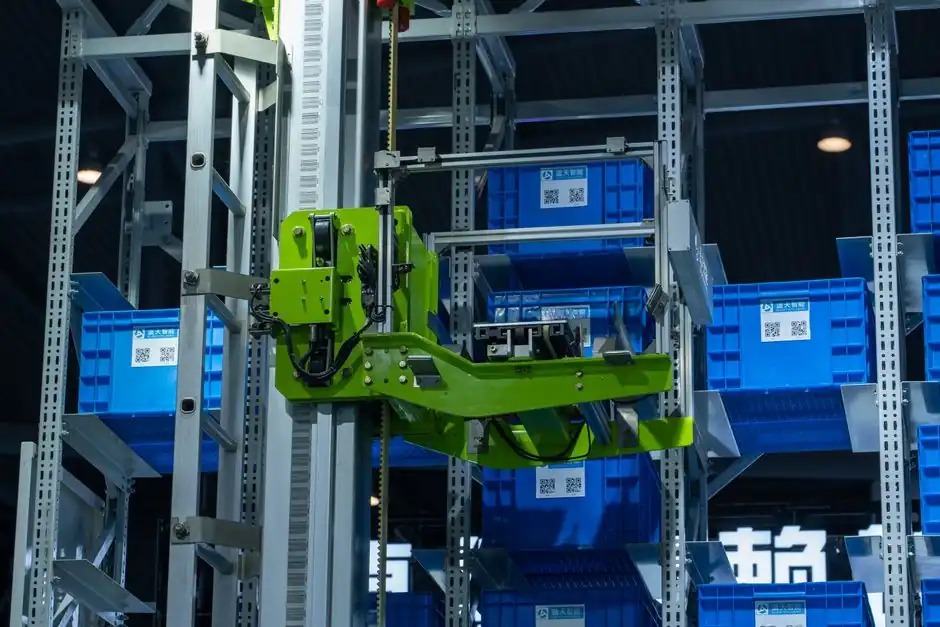
The 2026 AI build cycle is gated by four interlocking hardware chokepoints, advanced-node foundry and advanced packaging capacity at TSMC, high-bandwidth memory, grid and on-site power delivery, and the laser sources used for optical interconnects, that together determine how fast a new hyperscale campus can actually go live [S3].
None of the four is independently substitutable. As one industry observer put it in July 2026, the worst one gates demand for all the others; a data center cannot be commissioned with only three out of four of these bottleneck technologies scaling [S3]. A single missing ingredient, not a missing algorithm, is now the binding constraint on AI capacity.
Foundry and Packaging: The TSMC Funnel
Most leading-edge AI accelerators, whether designed by NVIDIA, AMD, or hyperscaler in-house teams, ultimately depend on TSMC's most advanced process nodes and CoWoS-style advanced packaging capacity, a concentration that creates a single industrial funnel for frontier compute [S4]. TSMC itself identified advanced packaging, not wafer production, as the industry's true bottleneck during 2025, directly constraining shipments of high-margin GPUs from NVIDIA and Broadcom [S5].
A leading-edge fab typically requires three to four years to build, plus additional time for tool installation and yield ramp, so the current capacity ceiling was locked in by capital decisions made before the 2025 demand surge [S4]. Reshoring commitments reflect this, with TSMC's Arizona investment raised to $165 billion, Intel committing $100 billion domestically, and NVIDIA announcing a $500 billion buildout plan, but new output from these projects will not materially relieve the 2026–2027 supply window [S5]. The U.S. CHIPS and Science Act has catalyzed over $630 billion in private investment commitments tied to this transition [S5].
HBM: Memory Becomes the Rate-Limiter
High-bandwidth memory has shifted from a secondary concern to a primary rate-limiter on AI accelerator shipments, with Micron publicly stating that the HBM shortage is expected to persist beyond 2026 [S5]. The constraint is amplified by allocation of general DRAM fab capacity to HBM stacking lines, reducing supply of conventional memory products across the broader electronics market and adding cost inflation that ripples into adjacent component pricing [S3][S5].
Each new accelerator generation stacks more HBM dies per package and demands higher per-stack bandwidth, so the industry's growth in usable tokens-per-watt depends on HBM throughput rising in lockstep with foundry output [S3]. When the HBM allocation is short, accelerator die that has cleared the fab is parked waiting for memory, which means packaging and memory capacity have to be co-planned, not procured independently [S3].
Power and Lasers: The Often-Overlooked Twin Constraints
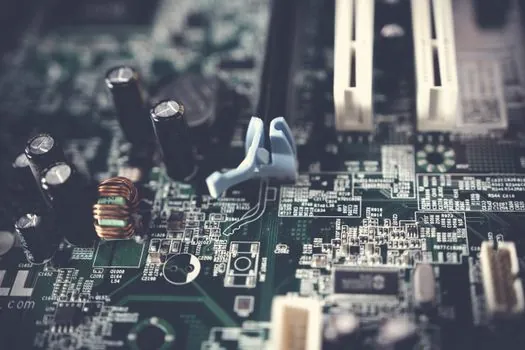
Grid and on-site power capacity has overtaken silicon as the most-cited reason new hyperscale campuses slip their commissioning dates, because AI training loads concentrate in regions whose transmission and generation buildout cycles run in years, not quarters [S3]. The response is architectural: hyperscalers are moving to vertical power delivery on the board to reclaim converter losses, and integrating high-bandwidth integrated voltage regulators so the xPU can run at peak efficiency and produce more tokens per watt delivered from a constrained grid feed [S3].
Inside the rack, optical interconnect is the second under-tracked constraint. Lasers for optical transceivers, needed to move data between servers in a rack and between racks, were not on most planners' roadmaps a year ago, but have become a fourth gating input as the transition from copper to optical accelerates through 2026 [S3]. Reliability of the rack-level power supply chain and the choice between a switching power supply topology and a dc power supply architecture now directly affects how many accelerators can be hosted per megawatt, which in turn sets the value of every additional HBM stack and every packaged die that TSMC ships.
EUV Lithography: The Single-Supplier Substrate
Even TSMC's capacity is downstream of a deeper single-supplier dependency: ASML's extreme ultraviolet lithography systems, which are the only commercially proven source for patterning the most advanced logic layers and have no qualified substitute at production scale [S4]. Each EUV tool costs hundreds of millions of dollars, takes years to manufacture, and represents a layered stack of specialized subsystems, which is why export controls on advanced lithography equipment have become one of the most consequential industrial-policy levers of the decade [S4].
The risk profile is therefore asymmetric. A fab can be insured against fire and earthquake, but EUV throughput, HBM stacking, packaging yield, and grid interconnect each gate the others, so loss of any one input in a given quarter halts the full stack [S3][S4]. For context on how downstream industries react when a single input becomes a binding constraint, the agricultural machinery parts shortage dynamics in 2026 show a similar pattern of cascade failure when one chokepoint part slips.
Server-Rack and Storage Implications
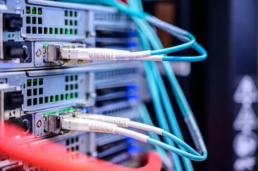
Because the four chokepoints co-gate output, the bottleneck visible at the rack level is not "too few servers" but "too few complete servers," a fully populated rack needing all of HBM, packaged accelerators, optical transceivers, and a viable power supply feed at the right voltage and current envelope. Hyperscalers have responded by pushing the supply chain toward co-design, with accelerator, HBM, packaging, optics, and power-conversion roadmaps negotiated together rather than procured independently [S3].
This shift is reshaping the storage layer of the rack as well. Higher accelerator density per rack increases the bandwidth demand on local storage rack tiers and on the pallet rack-style logistics flows that move finished servers into position, since a single delayed HBM lot can idle a whole staging lane for weeks. Rack-management interfaces are also re-architecting around serial server out-of-band consoles, because a partially populated rack now carries more diagnostic and telemetry responsibility per deployed accelerator.
Geopolitical Overlay and Industrial Policy
Chris Miller's February 2026 lecture at Carnegie Mellon University framed the situation in blunt terms: no single country today can produce even a moderately advanced chip on its own, and the leading-edge supply chain is therefore irreducibly multinational and exposed at each handoff between geographies [S2]. The same logic is driving the trillion-dollar reshoring cycle, with the U.S. CHIPS Act plus private commitments, the EU's push including Intel's outlined €80 billion European investment, and parallel programs in Japan, all attempting to shorten the most fragile legs of the chain [S2][S5].
Industrial policy, however, cannot reflow HBM, EUV throughput, or grid interconnect faster than its underlying engineering cycles allow. A fab takes three to four years to build; an EUV subsystem line takes longer; a transmission upgrade takes longer still, which is why the binding constraints of 2026 were effectively decided by capital and engineering decisions made in 2022–2024 [S4][S5].
Selection Criteria for Operators and Builders
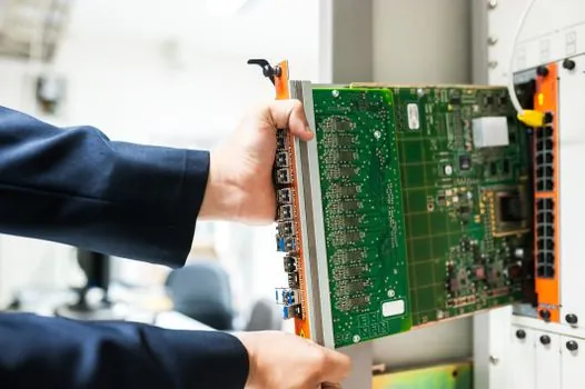
For operators planning a new AI campus in 2026, the practical decision is no longer which accelerator to buy but which accelerator allocation can be secured together with its HBM lot, its packaging slot, its laser allocation, and its grid interconnect date. Comparing the four chokepoints on procurement-risk criteria, TSMC foundry and packaging has the highest geopolitical exposure but the most established mitigation via reshoring; HBM has the clearest public timeline, with tightness flagged through 2026 and beyond; optical lasers have the fastest potential to scale if emitter supply responds; and power has the longest lead time and the least substitutability [S3][S4][S5].
The engineering consequence is to over-spec power and cooling headroom, dual-source optical transceiver vendors where possible, hold strategic HBM buffer stock, and treat the dc power supply and rack-level distribution as design-critical rather than commodity. The next verifiable nodes to track are Micron's HBM capacity updates, ASML's EUV shipment guidance, TSMC's CoWoS output, and the queue depth at U.S. interconnect-application authorities, each of which sets a hard ceiling on what the others can deliver in the following quarter.