An AI accelerator built in 2026 crosses roughly ten distinct value-chain layers before it lands in a powered rack: front-end wafer capacity at 3 nm and 5 nm nodes, CoWoS-L 2.5D advanced packaging, HBM4 high-bandwidth memory stacks, GPU/ASIC silicon design, board and substrate assembly, NVLink/PCIe/PCIe-Gen6 fabric, 800G to 1.6T optical interconnect, rack-level integration (NVL36/NVL72), and finally power and cooling at the data-center boundary [S2][S3].
The 2025 "silicon shock" rewrote enterprise sourcing logic: TSMC publicly identified advanced packaging, not wafer fabs, as the binding bottleneck, while Micron Technology warned the HBM shortage would persist beyond 2026, shifting capex decisions toward physical supply and away from the cloud-utility assumption that defined 2021 to 2024 [S4]. The AI data center total addressable market is now projected to grow from $242B in 2025 to $1.2T by 2030, a five-times expansion, with roughly $700B+ in hyperscaler capex guided for 2026 alone (Amazon ~$200B, Google $175-185B, Meta $125-145B, Microsoft $110-120B) [S2].
Foundry layer: TSMC N3/N5 wafer starts and the packaging pivot
Wafer capacity at TSMC's N3, N4P, and N5 nodes remains the upstream gate, with accelerator wafer counts tracked quarterly by SKU and process node in the SemiAnalysis model, alongside every downstream capacity order [S3]. The pivotal shift in 2025 was TSMC's own disclosure that CoWoS-L advanced packaging had overtaken wafer fabs as the true chokepoint, because each Rubin, B200, or TPU v7 die must be bonded to multiple HBM stacks on an interposer before it becomes a usable accelerator [S4].
Reshoring has re-priced the front end: the U.S. CHIPS Act catalyzed over $630B in private investment, with Nvidia pledging $500B in U.S. capacity, TSMC raising its Arizona commitment to $165B, and Intel earmarking $100B for domestic expansion, while Intel's European plan adds an €80B anchor on the other side of the Atlantic [S4]. These fabs are not equivalent today, however, and the most advanced packaging still ships from Taiwan, which is why SemiAnalysis ships its supply-chain module broken out by both foundry process node and 2.5D packaging line [S3].
Memory layer: HBM3E to HBM4 stacks as the second chokepoint
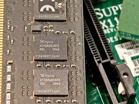
Every current-generation AI accelerator is memory-bound by HBM stack count, capacity per layer, and data rate, and SemiAnalysis tracks these fields for every SKU: HBM type, layer count, capacity per layer and stack, HBM stacks per package, total memory capacity, data rate, and memory bandwidth [S3]. The current binding constraints in 2026 are HBM4 ramp at SK hynix, Samsung, and Micron, where Micron's published view is that the HBM shortage will extend beyond 2026, lifting HBM ASPs and pulling memory suppliers to the top of the AI revenue table [S4].
The stack-count arms race is visible in the rack: Nvidia's GB200 NVL72 puts 72 GPUs in a single rack, each carrying multiple HBM3E stacks, and the Rubin generation lifts that to higher HBM4 capacities, while AMD's MI350X and MI450X push stack counts in the same direction; the resulting CoWoS-L interposer demand is what 2.5D capacity sizing in the SemiAnalysis model is built to forecast [S3][S2]. In a related decision map on AI rack cooling, the sensor and power-delivery pattern repeats at the facility layer.
Compute layer: GPU, custom ASIC, and the 75 to 86% share question
Nvidia's data center revenue hit $193.7B in FY2026 (+68% YoY), with H1 2026 AI accelerator share landing in a 75 to 81% band as custom ASICs scale; AMD sits at $16.6B in data center revenue for 2025 (+32% YoY) on MI300X, MI325X, MI350X, and the upcoming MI400, while Intel posts roughly $2B from Gaudi 3 plus the Crescent Island inference GPU (sampling H2 2026) and Jaguar Shores (2027) [S2].
The custom-ASIC counterweight is concrete: Broadcom and Marvell together control about 95% of the custom ASIC co-design market, with Google alone spending ~$8B/year with Broadcom on TPU development, and the TCO advantage for custom silicon at scale is 40 to 65% versus merchant GPUs, which is why AWS Trainium 1 to 6, Meta MTIA 200/300/400/500/600, Microsoft Maia 100 to 500, and OpenAI Gen 1/Gen 2 all appear in the SemiAnalysis SKU list alongside Google's TPU v4 to v11 [S2][S3]. On the China-domestic side, Huawei Ascend 910B/910C, Alibaba T-Head Zhenwu, Baidu Kunlunxin, Cambricon Siyuan 590/690, Biren, Hygon, Enflame, and MooreThreads form a parallel accelerator map that is tracked separately inside the model [S3].
Rack and fabric layer: NVL36, NVL72, and 10 to 36x more fiber
Rack-scale compute is the layer that has changed most between 2023 and 2026: Nvidia ships HGX, SXM, PCIe, NVL36, and NVL72 form factors, Google ships TPU v4 Pufferfish through v11 plus TIA and Merope custom parts, AWS ships Trainium 1 to 6 with Teton PD, PD Ultra, and PDS server types, and Meta ships MTIA 200 through 600, all of which are tracked down to the chip, server, and rack SKU level in the SemiAnalysis dataset [S3].
The fabric connecting those racks is now the third named chokepoint, after packaging and HBM: AI racks require 10 to 36x more fiber than traditional data-center builds, DAC and AOC lead times have exceeded 20 weeks, and the cable and optical interconnect market is projected to grow from $2.7B to $10.7B between 2024 and 2034 [S2]. TSMC's COUPE 1.6 Tbps optical engine is tracked by switch and XPU platform in the model, with attach rates mapped across Nvidia Quantum-3 and Spectrum families and across accelerator platforms, which makes optical attach one of the few areas where capacity orders can be forecast before a switch is announced [S3].
Data-center boundary: power, cooling, and grid as the fourth chokepoint
Once the rack leaves the OEM, the binding constraint moves to megawatts: a single 1 GW AI data-center campus is now a routine planning unit, and the SemiAnalysis model "stays at the chip-to-server level" while the OECD framework treats data-center availability, cooling limits, and grid access as the ultimate physical bottlenecks on AI deployment [S9][S4]. Nvidia's Vera Rubin platform being ARM-exclusive is the design tell that power-per-rack, not FLOPS-per-die, is now the limiting variable, with ARM server share moving from 5% in 2020 to ~20% in 2026 on 30 to 60% energy-efficiency gains [S2].
At the data-center layer, the supply chain stops being a chip problem and becomes a utility problem: hyperscaler capex guidance of ~$700B+ in 2026 is increasingly spent on substations, transformers, and behind-the-meter generation rather than on silicon, and the OECD notes that power, cooling, and grid access now determine deployment pace more directly than wafer output [S9][S2]. A practical example of the same physical-resource logic appears in heavy-equipment duty cycles, where the limiting step is not the prime mover but the surrounding cycle.
Who this supply chain is for, and where it breaks
This ten-layer map is for hyperscaler capacity planners, foundry and OSAT business-development teams, HBM and optical-component product managers, and any procurement engineer sizing 2026 and 2027 AI builds, and it is not useful for end-user model buyers, who should consume AI as a service and skip the layers entirely. The four named chokepoints, in order, are CoWoS-L 2.5D advanced packaging, HBM4 stack supply, 1.6 T optical interconnect, and grid power, and a sourcing plan that hedges any one of them while leaving the others single-sourced will still fail on the unhedged layer [S3][S4][S2].
The clearest leading indicators for 2027 are: (a) HBM4 capacity disclosures from SK hynix, Samsung, and Micron in the December 2026 and March 2027 quarters, which set the ceiling on Rubin Ultra, MI500, and TPU v11 volumes; (b) TSMC COUPE 1.6 Tbps optical engine attach rates by platform, which signal whether the interconnect gap is closing; and (c) the first 1 GW campus energization dates disclosed by the four U.S. hyperscalers, which set the outer envelope for accelerator absorption [S3][S2]. Each of these is a publicly trackable signal, not a forecast, and the SemiAnalysis Accelerator and HBM model is the dataset that ties them back to the SKU-level wafer starts that produce the silicon in the first place [S3].
The underlying component specifications are covered under pallet rack, storage rack, and power supply.