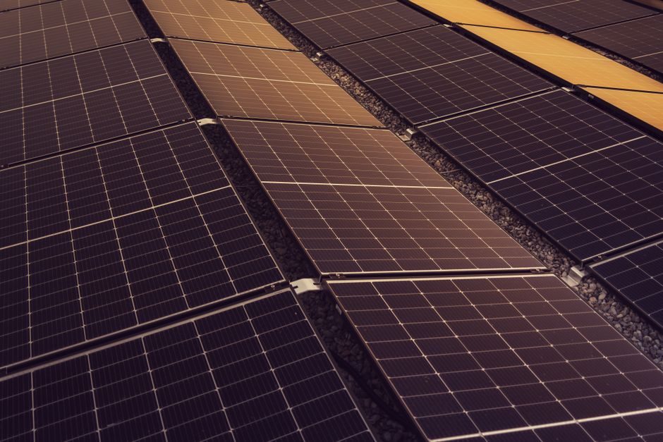
Interdigitated back contact (IBC) silicon cells reach 21.3% efficiency by relocating both emitter and contacts to the rear of an n-type wafer, eliminating front-side optical shading and freeing the front surface for full passivation and anti-reflection coating [S1].
The IBC route — developed at Stanford in the 1980s — uses boron diffusion for the rear p+ emitter, an n+ back-surface field, screen-printed rear metal electrodes firing through SiO2 contact openings, and a pyramid-textured front under SiO2 passivation, making it a credible high-efficiency platform for large-scale production [S1].
Process Flow and Critical Steps for Rear-Emitter IBC Cells
IBC fabrication begins with saw-damage etch removal on an n-type Czochralski wafer, followed by wafer cleaning, front-surface pyramid texturing, thermal SiO2 growth, boron diffusion to form the rear p+ emitter, phosphorus diffusion for the rear n+ BSF, rear-side contact opening through the oxide, and screen-printed silver metallization with co-firing, with paste deposit weights verified by inline load cell module feedback [S1].
Because the p-n junction sits on the rear, front-surface recombination dominates cell losses; an SiO2 passivation layer doubles as anti-reflection coating and as a front-surface field that repels minority carriers, while rear SiO2 suppresses back recombination and reflects long-wavelength photons to lift short-circuit current [S1]. Screen-printed point contacts through the oxide cut the metal-silicon contact area, suppressing contact-interface recombination and simplifying module-level cell interconnection [S1].
For plant engineers evaluating IBC lines, the practical spec envelope includes: p-type emitter sheet resistance in the 60-120 Ω/sq range achievable by boron diffusion, SiO2 passivation thickness tuned to ~75-110 nm for the anti-reflection peak near 600 nm, and rear metallization widened to reduce series resistance without front-side shading penalties [S1].
Bulk-Heterojunction Polymer Cells as a Solution-Processed Alternative
Polymer bulk-heterojunction solar cells (BHSC) use a phase-separated donor-acceptor active layer that is solution-coated, gravure- or slot-die-printed, or roll-to-roll processed under pressure transmitter-monitored coating windows, hitting power conversion efficiencies above 5% — competitive with amorphous silicon on flexible substrates [S2].
PCE is defined as P_solarcell / P_light = (j_SC · U_OC · FF) / P_light, where FF is the fill factor U_mp·j_mp / (U_oc·j_sc), and is limited by absorption profile, carrier mobility, active-layer morphology, and electrode work-function alignment [S2]. Scharber et al. and Dennler et al. project solution-processed PCE above 10%, with BHSC around 6% already demonstrated in lab cells using solvent additives to control donor-acceptor nano-morphology [S2].
Processing additives — solvent composition, solution concentration, deposition atmosphere, and process temperature — govern the nano-morphology and efficiency of bulk-heterojunction solar cells, with balanced miscibility and high crystallinity in the donor-acceptor blend as materials-engineering targets that improve FF and U_OC together [S2].
Comparison of Main Cell Architecture Options on Engineering Criteria

Engineers picking a cell platform for a 2026 line build normally compare crystalline silicon IBC, crystalline silicon PERC/PERT, and polymer BHSC on four criteria: efficiency, manufacturability, environmental load, and form-factor flexibility. [S1]
IBC silicon delivers 21.3% efficiency with mature screen-printed metallization, multi-step high-temperature diffusion, and rigid wafer form factor; PERC sits a few absolute points lower but with shorter, lower-cost process flows; BHSC is below 10% PCE in production-class cells but is the only platform compatible with roll-to-roll, flexible, lightweight, and large-area coating lines [S1][S2].
Material Properties That Drive Wafer and Absorber Choice
Monocrystalline silicon has 14 electrons per atom and a near-ideal band gap around E_g = 1.12 eV that efficiently absorbs photons near the band edge; intentional doping with phosphorus (n-type) or boron (p-type) tailors conductivity, while silicon's abundance, non-toxicity, and low unit cost keep it the dominant PV substrate [S3].
At short ultraviolet wavelengths, silicon absorbs strongly; at longer visible and near-IR wavelengths absorption weakens, which is precisely why IBC cells pyramid-texture the front, apply an anti-reflection coating, and reflect long-wavelength light from the rear SiO2 to recover current [S1][S3].
Process tolerance windows for IBC include: phosphorus gettering and emitter diffusion temperatures of 800-950 °C verified by a multifunction process calibrator, screen-print firing peaks near 700-800 °C with controlled ramp rates to avoid wafer warpage, and HF-based post-firing cleaning to remove residual glass frit from the rear point contacts [S1].
Limitations, Failure Modes, and Where Each Platform Does Not Fit

IBC's rear-junction design makes the front surface the dominant recombination surface, so any passivation-layer pinhole, residual organic contamination, or pyramid-texturing non-uniformity translates directly into U_OC loss; fabs running IBC must hold front-surface recombination velocity well below the 1000 cm/s range typical of unpassivated silicon [S1].
BHSC active layers degrade under oxygen, moisture, and UV exposure, and large-area roll-to-roll coating struggles with thickness uniformity and donor-acceptor phase separation; the platform is therefore a poor fit for utility-scale, 25-year-warranty installations despite its flexible-substrate advantage [S2].
Bath-salt-substituted absorbers are a recent lab-scale development; until pilot-line data validates stability, throughput, and yield, specifying engineers should treat them as a research-grade option rather than a drop-in replacement for established CdTe, CIGS, or perovskite stacks [S5].
Sourcing Signals and Standards Reference
Reliable IBC manufacturing data sources include the original Stanford back-point-contact analyses and current ScienceDirect topic pages; for BHSC, peer-reviewed reviews of bulk-heterojunction morphology and additive engineering set the baseline for any efficiency claim [S1][S2][S4].
Silicon substrate and doping behavior, including the 1.12 eV band gap that anchors PV device physics, is documented in standard photovoltaic engineering texts and is the reference for any custom line's material-purchase specification [S3].
Engineers sourcing IBC tools, BHSC coating lines, or alternative-absorber pilot equipment should track three 2026 signals: published fab-level IBC average efficiency above 24% on n-type wafers, the first commercial-scale roll-to-roll BHSC line, and a peer-reviewed stability dataset for the bath-salt absorber family — see also the solar inverter cell-pairing and audit anchors for downstream module-level integration constraints, and the sodium-ion cell manufacturing process map for adjacent dry-room and coating-line process analogies that translate across PV and battery production.