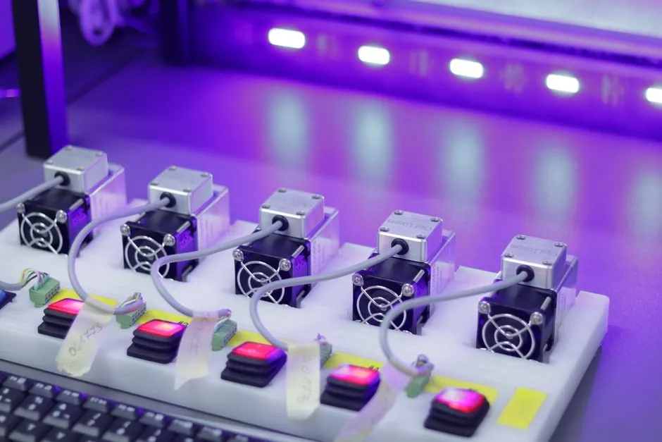
LED chip and module production lines draw on a common core of front-end and back-end semiconductor equipment, so the same selection logic that drives fabs also governs LED fabs: throughput, yield, mean time between assists, and SECS/GAM compliance [S3]. The wider semiconductor manufacturing equipment market was valued at USD 166.35 billion in 2025 and is projected to reach USD 344.36 billion by 2032, expanding at an 11.0% CAGR from 2025 to 2032, with Asia Pacific holding the largest regional share [S2].
An LED line typically bundles epitaxy, lithography, deposition, dicing, bonding, testing, and aging, plus downstream optical-lens moulding, SMT placement, and light-curing encapsulation [S1][S5][S6]. Process engineers buying kit in 2026 should treat each station as a spec object, not a brand decision, and weigh interface conformance under SEMI EDA standards early [S3].
What counts as LED manufacturing equipment
LED manufacturing equipment covers the full chain from epitaxial wafer growth to packaged, binned, and aged emitters. At the front end, MOCVD reactors deposit GaN-on-sapphire or GaN-on-SiC layers; at the back end, scribe-and-break systems (DPS and DBM), chip testers, can testers, aging systems, and visual inspection stations turn finished die into tested lamps [S4].
Downstream of the chip, lens moulding, light-curing encapsulation, and SMT pick-and-place turn tested LEDs into modules, with PMMA optical lenses commonly injection moulded to customer spec for street-light, spotlight, and COB form factors [S6]. The line is short relative to a logic fab, but the precision, ESD, and binning requirements are similar, so SEMI smart manufacturing standards for equipment data acquisition, SECS, and GEM are routinely cited by LED tool vendors [S3].
Front-end stations: MOCVD, lithography, deposition, metrology
MOCVD is the throughput-defining step on a GaN LED line; reactor count, wafer size (2-inch, 4-inch, 6-inch), and uniformity drives capex. Photolithography aligns the p-contact and ITO layer, while PECVD or sputter deposition lays down the transparent current-spreading layer; inline metrology and wafer surface conditioning stations sit between process steps to keep drift in check [S2][S4].
Selection criteria at this stage: wafer size compatibility, throughput in wafers per hour, temperature uniformity across the susceptor, and cleanroom class. Equipment data acquisition under the SEMI smart manufacturing standards programme, including EDA (Equipment Data Acquisition), DAQ, and the legacy SECS/GEM interfaces, lets a fab plug the tool into a host MES for traceable per-wafer genealogy [S3].
Back-end stations: scribe, dice, bond, inspect, age

Once epi is qualified, scribing and breaking (DPS for diamond-pen scribe, DBM for DBG-style) separate the wafer into individual die, after which wire bonders (gold or copper) interconnect the die to the leadframe, and can sealers close the package [S4]. Chip and can testers parametric-test Vf, IV, dominant wavelength, and luminous flux, then aging systems burn-in parts at elevated current and temperature to flag infant mortality [S4].
Criteria at back end: bond pull strength in grams, placement accuracy in micrometres, tester parallel-site count, and aging chamber channel count. Visual inspection stations close the loop, catching die cracks, bond lift, and phosphor-coating defects that would otherwise pass electrical test. For lines that build COB and street-light modules downstream, PMMA optical lens moulds and light-curing encapsulants seal and shape the output beam [S5][S6].
Options and trade-offs by station type
For scribing, diamond-pen scribing (DPS) is the lower-cost route for thin sapphire, while DBG (dice-before-grind) suits thicker SiC and GaN-on-SiC carriers. Wire bonding splits between gold ball (high reliability, higher material cost) and copper wedge or copper ball (lower cost, tighter process window). Aging systems range from small benchtop burn-in racks to multi-channel environmental chambers with 500+ sockets, and the choice scales with binning strategy [S4].
For optical lens moulds, single-cavity steel moulds suit low-mix runs, while multi-cavity moulds with family tooling cut piece price at the cost of cycle-time tuning. UV/visible light-curing systems can be flood, focused-beam, or conveyor, with conveyor systems typically chosen for inline tacking of lenses to housings at cycle times below 30 s per part [S5]. Across all of these, SECS/GAM conformance and EDA-compliant data logging shorten integration time and ease recipe transfer between sites [S3].
Who benefits and who should not buy

Buyers who benefit: integrated LED module makers running 24/7 lines with MES-controlled recipe download, OSAT-style contract packagers, and tier-2 lighting brands that want in-house chip-to-module control for street-light, COB, and horticultural SKUs [S1][S6]. Lines that should not buy a full in-house toolchain: small custom-sign shops that only need finished LED strip and channel-letter modules, since unit cost from a contract packager beats capex amortisation below roughly 100,000 units per year [S1].
For new entrants, the practical alternative is to contract the epitaxy and chip test, keep module-level SMT, light-cure encapsulation, and final QC in house, and add capacity only when binning yield and order book justify it. Buying a turnkey line on lease terms is a poor fit if the customer's primary products are short-run custom signs rather than mass-produced emitters, because scribe-and-break and aging test cannot be amortised across a small SKU count [S1][S4].
Standards, sourcing, and integration signals
Three standards bodies dominate the interface question. SEMI's smart manufacturing programme owns SECS (SEMI Equipment Communications Standard), GEM (Generic Model for Communications and Control of Manufacturing Equipment), and the more recent Equipment Data Acquisition (EDA) standards that let tools stream per-wafer data into an MES [S3]. Optical and metrology stations should be cross-checked against the relevant IEC laser-safety and ESD-control norms, even where the vendor does not lead with a specific standard number.
Sourcing signals worth tracking: vendor publication of SECS/GAM conformance certificates, EDA implementation guides, and a public MTBF or MTTR figure. Process engineers building or upgrading an LED line can benchmark broader capex cycles against the 11.0% CAGR in adjacent semiconductor equipment through 2032, which keeps tool lead times tight for high-end MOCVD and wire bonders [S2]. Two trackable 2026 signals: SEMI standards releases in the EDA family, and new ASMPT/K&S/SECA-equivalent bonders, MOCVD tools, and aging systems entering Asia Pacific service networks. For guidance on adjacent selection problems, see heat pump manufacturing equipment: a spec-driven line selection guide and proximity sensor selection guide: inductive vs capacitive vs magnetic in 2026.
For the relevant spec sheets and selection criteria, see additive manufacturing material, linear guide, and ndt equipment.