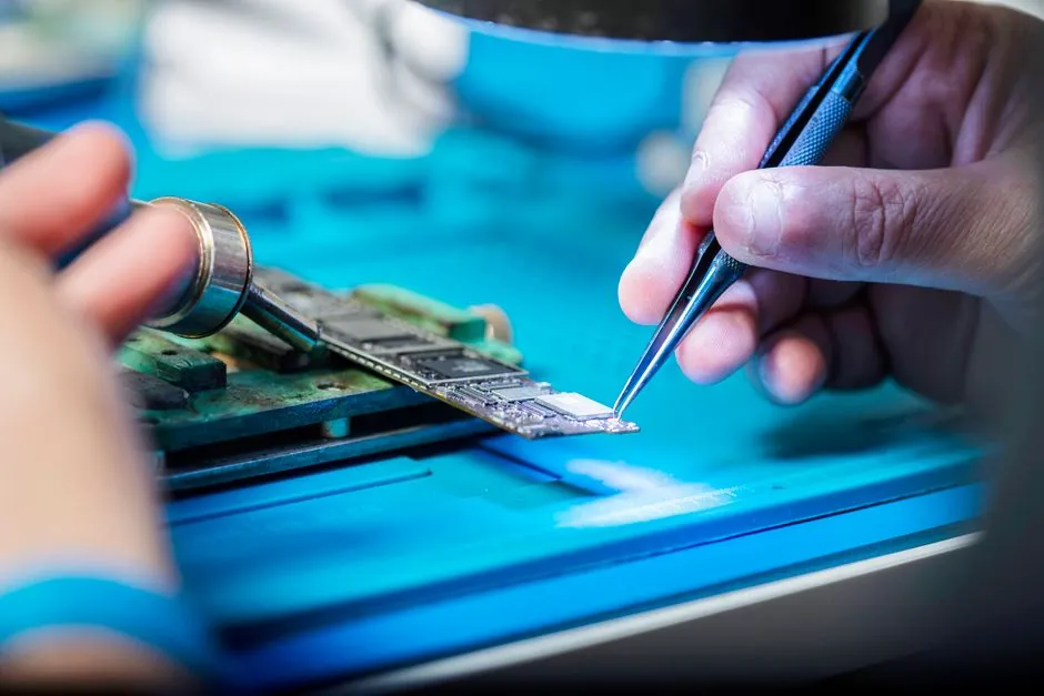
A MEMS sensor is a Micro-Electro-Mechanical System that combines a microscopic mechanical structure (a diaphragm, cantilever, comb-finger, or proof mass) with electronic readout on a single silicon die, then encloses the pair in a protective package [S1][S3]. Every commercial device carries the same five-stage bill of materials: raw wafer, MEMS microstructure, ASIC die, interconnect stack, and first-level package housing.
For process engineers, the BOM is where MEMS reliability is won or lost. The 2021 review of MEMS actuation and sensing mechanisms identifies sensitivity, resolution, accuracy, limit of detection, and response/recovery time as the parameters that translate material choice into field performance [S1]. Selection at the component level therefore drives datasheet numbers, not the other way around.
Silicon, glass, and the wafer-level substrate
Single-crystal silicon is the dominant MEMS substrate because it carries a well-characterized Young's modulus (~130-188 GPa across crystal orientations) and is compatible with batch-fabrication CMOS lines [S1]. Wafer-level processing splits into surface micromachining, which builds structures from patterned thin films, and bulk micromachining, which etches into the silicon crystal itself using wet or dry chemistries [S2]. Bonding closes the device: field-assisted thermal bonding, thermal fusion bonding, and eutectic bonding are the three production workhorses for sealing cavities and stacking dies [S2].
Borosilicate glass (Pyrex-type) is the second most common substrate, chosen because its thermal expansion coefficient is closely matched to silicon, which reduces residual stress across temperature cycling. Residual stress in thin films is a documented failure driver: poor adhesion plus trapped stress causes delamination of the microstructure [S2]. Engineers specifying a BOM should treat wafer flatness, TTV, and bow as incoming-inspection items, not as foundry-side guarantees.
MEMS microstructures: diaphragm, cantilever, comb-finger, proof mass
The sensing element is the moving structure that converts the physical input into a measurable signal. A MEMS pressure sensor uses a diaphragm and a fixed electrode as a variable capacitor; deflection under pressure changes the gap and produces an output [S6]. An automotive acceleration sensor uses interdigitated, comb-shaped silicon fingers that interlock across a proof mass; inertial force moves the mass and changes the capacitance between finger pairs [S8].
Geometry and transduction principle both flow from the BOM. Capacitive, piezoresistive, piezoelectric, electromagnetic, and electrothermal mechanisms each demand different materials on the die [S1]. A piezoresistive pressure sensor adds doped silicon resistors diffused into the diaphragm; a capacitive version adds only metal electrodes and a sealed cavity. Specifiers should match the transduction principle to the measured variable before locking the wafer process, not after.
ASIC die and the transducer interface
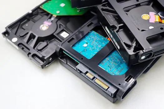
Every MEMS sensor ships with a companion ASIC on the same package, sometimes on the same die. The ASIC performs signal conditioning, analogue-to-digital conversion, temperature compensation, and bus output (I2C, SPI, or analogue) [S3]. In a first-level package the MEMS element and the ASIC are placed side by side or stacked, then linked by bond wires thinner than a human hair [S3].
The ASIC dictates power, noise floor, and interface protocol, so the BOM line for the ASIC is rarely a generic "signal conditioning IC". For an industrial pressure transmitter built around MEMS, the ASIC choice governs whether the device speaks 4-20 mA + HART, IO-Link, or a digital automotive bus. Engineers sourcing MEMS modules for displacement sensor or capacitive sensor assemblies should treat the ASIC part number as a binding input, not a swappable commodity.
Interconnect: bond wires, solder bumps, through-silicon vias
Wire bonding is still the highest-volume interconnect because it is the lowest-cost route and tolerates mixed chip sizes. Gold and copper are the standard wire metallurgies, with aluminium used on aluminium bond pads. The NASA COTS-MEMS study notes that MEMS packages must simultaneously protect the die from contamination and, in sensor variants, expose the microstructure to the measurand [S2]. This dual requirement is what makes MEMS packaging harder than standard IC packaging.
For higher-density designs, flip-chip solder bumping and through-silicon vias (TSVs) replace wire bonds, but each adds cost and process risk. Solder bumps introduce lead-free metallurgy constraints (SAC305 and variants) and require underfill, while TSVs demand extra masking, etch, and copper-plating steps. The reliability trade-off is straightforward: more interconnect density buys electrical performance and shrinks package height, at the cost of additional BOM line items and qualification effort.
Package housing: ceramic, plastic, metal
Package reliability depends on the housing material class: ceramic, plastic, or metal [S2]. Plastic packages, transfer-molded with epoxy moulding compound, win on cost and volume, and are the workhorse for consumer and mobile MEMS.
The Bosch packaging team describes the trade-off plainly: every adhesive, substrate, and moulding step is engineered per product because MEMS reacts to the slightest mechanical stress [S3]. For an accelerometer or pressure sensor with a media port, the housing must expose the die to the environment while keeping moisture and ionic contamination out. The BOM line for a gel-filled port, a stainless-steel barrier, or a sintered filter is therefore a sensor function, not a packaging accessory.
Bill of materials, end to end
A representative MEMS sensor BOM breaks into five blocks, each tied to a documented failure mode: [S1]
(1) Wafer and substrate: single-crystal silicon wafer, optional borosilicate glass cap wafer, bonding interface (anodic, fusion, or eutectic). Failure mode: residual stress and delamination [S2]. (2) MEMS microstructure: silicon diaphragm, cantilever, comb-finger, or proof mass; metal electrodes; doped piezoresistors where applicable. Failure mode: fatigue, stiction, overload fracture. (3) ASIC die: CMOS signal conditioning, ADC, memory, bus interface. Failure mode: ESD, latch-up. (4) Interconnect: gold, copper, or aluminium bond wires; solder bumps; or TSVs. Failure mode: wire sweep, bond pad cratering, electromigration. (5) First-level package: leadframe or substrate, die-attach adhesive, moulding compound, media port, gel or filter, optional metal or ceramic lid. Failure mode: package crack, moisture ingress, port blockage.
Engineers building industrial sensor assemblies, including construction machinery and equipment telematics and lighting equipment and electric lamps drivers, can reuse this five-block template to audit any MEMS supplier's datasheet against the same failure list.
Transduction principles and material demand
Each topology shifts the BOM. Capacitive sensors are the cheapest and lowest-power; piezoresistive sensors trade simpler readout electronics for higher temperature sensitivity; piezoelectric sensors need a charge or voltage amplifier but draw essentially zero quiescent current. The choice cascades into the package: a piezo film is sensitive to contamination, so the cavity is sealed more aggressively than for a capacitive device.
What to verify on a MEMS supplier's BOM
Five checks separate a working BOM from a fragile one. First, confirm the wafer-level bonding interface and the hermeticity class, since that line determines long-term drift in media-exposed devices [S2]. Second, confirm the die-attach adhesive and its cure profile, because MEMS die are sensitive to cure-induced stress [S3]. Third, confirm the moulding compound and the post-mold cure, since absorbed moisture is a primary failure driver in plastic packages. Fourth, confirm the media-port filter or gel specification, including pore size and material compatibility with the target media. Fifth, confirm the bond-wire metallurgical system and the bond pad finish, because galvanic corrosion at the pad is a known reliability risk in humid environments.
Engineers comparing MEMS accelerometer or pressure sensor offers should run these five checks against every candidate. The cheapest unit price usually reflects a thinner BOM on one of these five lines, not a process breakthrough. For a deeper dive into upstream material supply, the MEMS sensor raw material sourcing reference covers silicon, piezo films, metals, and polymers in detail.
Limits and failure modes engineers should plan for
No MEMS datasheet removes the need for system-level derating. Three constraints recur across vendors. Shock survivability: high-shock events (thousands of g) can fracture the microstructure or bond wires, especially in small proof-mass designs. Temperature range: piezoresistive and capacitive sensors drift with temperature; the ASIC compensates, but only across a specified range, typically -40 °C to +125 °C for automotive and -20 °C to +85 °C for consumer. Media compatibility: the media port, gel, and any exposed metallisation must be specified against the actual process fluid, including water vapour, hydrocarbons, and corrosive gases [S2].
Stiction, the tendency of microstructures to adhere after release, is a wafer-process artefact that can survive into the field if humidity control during packaging slips. Hermeticity testing (fine and gross leak) is therefore not optional for safety-relevant MEMS. The same logic drives AEC-Q100 qualification in automotive and IEC 60079 series compliance for MEMS used in hazardous-area equipment, with the lamps and light fittings and industrial-sensor markets inheriting the same qualification burden.
These three indicators will define the next 12-18 months of MEMS sourcing, and each ties back to a specific block in the five-block BOM outlined above.