
OLED panel output in 2026 is bounded upstream by GEN 8.6 evaporation capacity, linear evaporation sources, and FMM (fine metal mask) inventory, and bounded downstream by smartphone, IT, and automotive display module integration [S1].
Each of these gates a different vendor, lead-time, and unit-cost profile [S2].
Upstream Stack: Vacuum Coating, Evaporation and Precision Coating Tooling
Vapor deposition in 2026 spans single-substrate magnetron sputter lines, in-line magnetron continuous sputter systems, and horizontal point-source evaporation tools, all targeting films for perovskite PV, flexible display, and新能源 applications [S4]. Magnetron sputter systems running a 公自转转架 (planetary rotation) carrier deliver uniform deposition on hard coatings, hydrogen bipolar plates, and decorative parts, with target-set flexibility for reactive or elemental sputtering depending on the film function [S4].
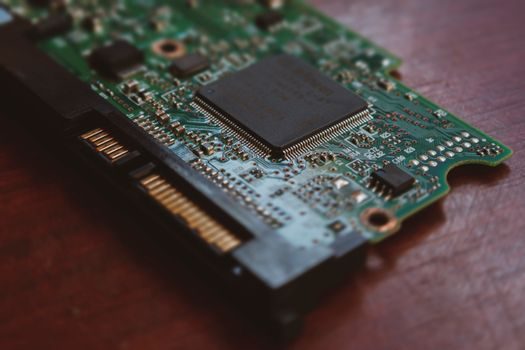
Equipment choice inside the OLED tool chain maps directly to device layer: ITO (indium tin oxide) anode deposition typically sits on DC-magnetron sputter with the substrate moving at a controlled linear speed, while organic emissive layers require linear evaporation sources inside a GEN 8.6 vacuum chamber held at roughly 10⁻⁶ Pa base pressure. The compact, highly-integrated form factor of newer sputter tools is what allows a Tier-1 panel fab to drop 30–40% floor space versus 2022-vintage systems [S4].
Midstream Panel Manufacturing: GEN 8.6, Flexible Substrate and Encapsulation
AMOLED midstream capacity in June 2026 is dominated by GEN 8.6 fabs cutting mother glass at roughly 2250 × 2600 mm, and GEN 6 flexible lines cutting 1500 × 1850 mm polyimide substrates. The two formats are not interchangeable: GEN 8.6 is optimised for TV, monitor, and IT panel throughput; GEN 6 is the workhorse for smartphone and foldable panel batches where the mother glass is laser-cut into hundreds of small-format units [S3].
TFE stack architecture has converged across major panel makers on a dyad of Al₂O₃/acrylate alternating layers, with three to five dyads typical for water-vapour transmission rate (WVTR) targets under 10⁻⁶ g/m²/day at 60 °C / 90 % RH. Where moisture sensitivity is extreme, manufacturers add a getter desiccant inside the encapsulation dam — a hybrid stack that pushes the effective WVTR one decade lower without changing the sputter recipe [S2].
Downstream Module Integration: Driver ICs, Touch Films and Bezel-less Stack-ups
Downstream display module assembly in 2026 is increasingly driven by COG and COP bonding yields rather than by OLED panel availability. COP lets the driver IC sit on a flexible polyimide tail that bends behind the display, enabling a 0.8 mm to 1.2 mm chin-bezel reduction versus legacy COG designs; the trade-off is COP-tool CAPEX and a tighter bonding-pad pitch tolerance in the 18 µm range [S1].
On-cell touch has become the default for mid-range smartphone panels because it eliminates one interlayer film, drops module thickness by roughly 50 µm, and improves optical transmittance by 4–6 % relative to add-on GFF (glass-film-film) stacks. Engineers validating touch performance should pin a ΔC/CT (delta capacitance, capacitance/target) spec on the touch-Si vendor's datasheet, not on the panel-maker's marketing sheet [S3].
Spec Levers for 2026 Sourcing Decisions
Three spec levers determine whether a given OLED module is fit for the application in 2026: peak luminance (cd/m²), operating-temperature range, and the lifetime metric LT₉₅ (time to reach 95 % of initial luminance). Mainstream smartphone panels target 1000–1500 cd/m² peak, automotive centre-stack displays target 800–1200 cd/m² with an operating range of −40 °C to +85 °C, and TV panels trade peak brightness for LT₉₅ lifetime of 30 000 h or more [S2].
Material and process gaps are the realistic constraints, not headline spec sheets. Tandem OLED stacks with two emission layers (often a fluorescent blue + phosphorescent yellow/green) roughly double the LT₉₅ lifetime at the cost of about 1.4× the deposition cycle time, and any midstream process re-tuning extends downstream module lead times by 8–12 weeks in 2026 capacity. Engineers should treat tandem-stack modules as a separate BOM line, not as a drop-in [S4].
Cross-Industry Linkage: Optical Fibre, Photovoltaic and Display Equipment
The optical-fibre industry is being pulled into a digital-economy cycle alongside upstream and downstream display and semiconductor manufacturing, with vendors positioning all-optical network ecosystems as the integration fabric for smart factories and 5G backhaul [S3]. Equipment vendors serving both OLED panel coating and optical-fibre preform deposition share common vacuum, sputtering, and precision-metrology platforms, which is why a single OEM can ship both a sputter line for ITO and a similar-source platform for fibre preform jacket layers [S3].
This shared-vacuum-toolbase is also why perovskite-PV scaling interacts with OLED midstream capacity: the same linear evaporation source set used for organic emissive layers can deposit perovskite absorber stacks, and the same ALD (atomic layer deposition) chamber used for TFE inorganic layers can be repurposed for perovskite barrier layers. A sourcing team that has already qualified a vendor for OLED TFE has a head start on perovskite-PV barrier qualification [S4].
Risk Map: Lead Times, Sourcing Bottlenecks and Qualification Gates
The tightest 2026 bottlenecks in the OLED chain are not the OLED emitters themselves but the FMM shadow masks used for fine-pixel patterning, the linear evaporation sources inside GEN 8.6 chambers, and the driver-IC COG/COP bonding lines. Each is single-digit-supplier concentrated, and a fab-side audit of those three nodes predicts 12-month lead-time exposure more reliably than any public forecast [S1].
Buyers should track three trackable signals through the rest of 2026: GEN 8.6 utilisation rate at the top-three panel makers, FMM shadow-mask inventory weeks-of-supply, and driver-IC COG/COP bonding line yield at the Tier-1 OSAT (outsourced semiconductor assembly and test) vendors. Movement on any of those three is a leading indicator of whether a planned 2026 OLED module launch will hold its original delivery slot. For related engineering and supply-chain context, see our OLED panel supply 2026 sourcing analysis and our power-semiconductor production spec cut for adjacent driver-IC capacity context.
For component-level specifications, see pressure transmitter, flow meter, and industrial valve.