Power semiconductors are the switching and converting building blocks behind every inverter, UPS, traction drive and renewable tie-in; the device families that matter in 2026 are silicon IGBTs and MOSFETs, silicon-carbide (SiC) MOSFETs/modules, and gallium-nitride (GaN) HEMTs, each produced on its own process line [S3][S5].
What separates "power" devices from logic ICs is current and voltage headroom: power devices are built on thick, lightly-doped epitaxial layers, large cell pitches, and packaging that can sink kilowatts of heat, whereas logic is built on thin SOI/bulk Si for speed [S3]. A 1.7 kV full-SiC module released in 2021 cut switching loss by about 30% versus the existing Si IGBT module it replaced [S1].
Wafer and epi process: where the breakdown voltage is set
Breakdown voltage in a power device is set by the drift-region thickness and doping, which is why power wafers are grown as epitaxial layers on heavily-doped substrates rather than being diffused like logic transistors [S3]. A 1.7 kV class device needs a drift region tens of microns thick with resistivity tuned so the electric field stays below silicon's critical field of roughly 0.3 MV/cm at the rated blocking voltage.
SiC and GaN change the math: SiC has a critical field around 3 MV/cm, an order of magnitude above Si, so a 1.7 kV SiC MOSFET uses a thin drift region (about 10× thinner than a silicon IGBT of the same rating), which is exactly why switching loss drops ~30% on Hitachi's full-SiC module [S1]. Production lines for SiC and GaN run hot — SiC epitaxy typically uses 1500–1700 °C susceptor temperatures, well above the 1100–1200 °C ceiling of a silicon epitaxial reactor.
Cell, gate and process modules: IGBT, MOSFET, HEMT side by side
An IGBT is a voltage-driven, four-layer (PNPN) device combining a MOSFET input stage with a bipolar output, giving low Vce(sat) at the cost of a tail current during turn-off; it dominates 600 V to 6.5 kV converters and is the workhorse of traction and motor drives [S5][S6]. A power MOSFET (Si planar or SiC trench) is a unipolar majority-carrier device, faster but with an Rds(on) that rises steeply with voltage rating, so it is preferred below ~900 V.
GaN HEMTs are lateral, normally-off enhancement-mode devices on SiC or Si substrates, prized for sub-200 V to 650 V high-frequency power conversion because of near-zero reverse-recovery charge. All three are built with the same basic CMOS-style flow — photolithography, implant, gate-oxide/dielectric deposition, metallization, passivation — but IGBTs add a thick field-stop and backside-metallization grind, and SiC/GaN lines add ion-implant activation anneals at 1600–1700 °C that a Si fab cannot do.
Back-end: packaging is half the electrical spec

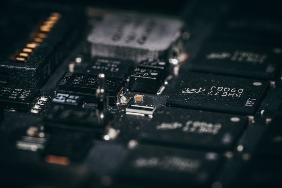
Packaging controls thermal resistance Rth(j-c), parasitic inductance, and isolation voltage; a great die in a poor package still fails as a 50 kHz switching node. Production lines use heavy copper leadframes or direct-bond-copper (DBC) Al2O3/AlN substrates, with three joining options: solder, silver-sinter, and Cu-Cu hybrid bonding [S6].
Ag-sinter die attach lets a SiC module run junction temperatures of 175–200 °C continuous versus the ~150 °C ceiling of a soldered Si IGBT, which is one reason Hitachi's 1.7 kV full-SiC module shows both the ~30% switching-loss cut and the durability improvement for traction/renewable duty [S1]. The back-end also adds wire bonds (Al, 200–500 µm) or copper-clip bonds, and overmolds or gel-potted housings that must pass IEC 60749 / UL 94 V-0 and isolation tests up to the module's rated Vrms.
Reliability gates: HTRB, HTGB, PC, and power cycling
Every automotive and industrial power device is qualified against a fixed stress matrix defined in AEC-Q101 (discrete) and AEC-Q104 (module). The four mandatory gates are HTRB (high-temperature reverse bias, typically 1000 h at max Tj and 80% of rated Vds), HTGB (gate bias, 1000 h at max Tj), H3TRB (biased 85/85 humidity), and power-cycling (ΔTj cycling up to 20 000 cycles) [S3].
Functional-safety and software ecosystems are increasingly part of the supplier spec: CISSOID ships ASIL-D certified software alongside its IPMs, IGBTs, and SiC inverter reference designs for e-mobility and high-power applications [S2]. For silicon-carbide modules, additional JEDEC JC-70 gate-oxide and short-circuit robustness tests are commonly written into vendor datasheets, since SiC's thinner gate oxide and higher dv/dt make the standard Si-only matrix insufficient on its own.
Who uses which family: a 2026 buyer cut
Below 200 V and a few kW — server 48 V, USB-PD chargers, telecom rectifiers, small motor drives — GaN HEMTs win on frequency and reverse-recovery loss. 400 V/800 V EV traction and 1500 V solar strings are the SiC MOSFET and SiC module battleground, where 30% lower switching loss directly translates to either longer EV range or higher inverter kW/kg [S1]. Above 1.7 kV, in HVDC, rail traction, and large wind converters, the Si IGBT (often press-pack, with optional SiC anti-parallel diode co-pack) is still the only fully-mature choice, and Littelfuse/IXYS, Infineon, and Hitachi all maintain broad discrete IGBT and IGBT-module portfolios in this range [S1][S5].
Who should NOT chase SiC or GaN: low-volume industrial users buying 600 V motor drives at commodity prices, where Si IGBT modules remain the cost-optimized answer; the capex of a SiC line and the die-cost gap still close only at 1200 V and above for high duty cycle. Vendors such as Wuxi Unigroup Guoxin (紫光国微) and JSAB Technologies position around silicon-based power discrete and module design, fab, and packaging, with Wuxi Unigroup Guoxin's Wuxi Unigroup Microelectronics focused on power device R&D, fab processing, packaging, test and sales, while JSAB is led by an IEEE Fellow from HKUST and is the only IEEE Fellow in Greater China working on silicon-based power semiconductor research [S4][S8].
Production economics: what moves the die-cost curve
The two cost levers are wafer size and yield. Silicon power has moved to 200 mm and is piloting 300 mm; SiC is migrating from 150 mm to 200 mm substrates in 2025–2026, which alone trims die cost ~30% at constant yield because a 200 mm wafer yields roughly 1.78× the die area of a 150 mm wafer of the same thickness. GaN-on-Si runs on 200 mm CMOS-compatible lines, which is why its $/A figure looks closer to silicon at low voltage. [S1]
Yield losses in power lines come from three predictable sources: epitaxial defects (micropipes, basal-plane dislocations in SiC; V-pits in GaN), gate-oxide failures under HTRB, and die-attach voids that drive Rth(j-c) up and power-cycle life down. Vendors that bring the epi reactor, the fab, and the Ag-sinter back-end in-house (the Hitachi, Infineon, and ON Semi model) tend to dominate the automotive SiC auction cycle for that reason [S1]. For buyers, the practical read is that two otherwise-identical 1200 V SiC MOSFETs from different fabs can vary by 20–40% in $/A simply because one buys third-party epi and the other does not.
Standards, sourcing, and the spec sheets that matter
The standards that actually pin a power device on a BOM are JEDEC JESD22 / AEC-Q101 / AEC-Q104 for stress, IEC 60747 for discrete semiconductors, UL 1557 for power-module isolation, and IEC 61287-1 for railway power converters; a SiC or IGBT module aimed at traction must clear all four [S3]. For the buy side, the four numbers worth chasing on a datasheet are Vds/Vce (continuous, not pulsed), Rds(on) or Vce(sat) at the real gate drive (15 V SiC, 10–12 V Si, 5–6 V GaN), Eon+Eoff at 25 °C and 150 °C, and Rth(j-c) with the recommended mounting torque and TIM.
Trackable 2026 signals to watch: published 200 mm SiC substrate roadmaps from Wolfspeed, Resonac, and SICC, the second-generation 750 V to 1200 V SiC MOSFET gate-oxide revisions at Infineon and onsemi, and the move of 48 V server power into GaN at the 5–10 kW brick level. For related industrial spec cuts that share the same sourcing discipline — from bearing buying decisions to casting mold cost levers — the rule of thumb is identical: anchor the BOM on a datasheet number traceable to a published standard, not on a vendor brochure.
For component-level specifications, see power cable, power meter, and power mixer.