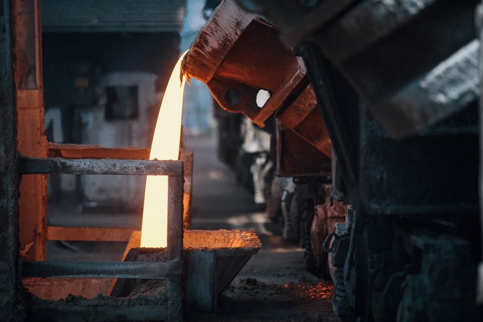
Four production routes account for essentially all merchant polysilicon: the Siemens trichlorosilane (TCS) process, the fluidized-bed reactor (FBR) silane route, upgraded metallurgical-grade (UMG) refining, and small-volume semiconductor-grade processes such as float-zone refining and polysilicon MEMS deposition [S1][S3].
The Siemens TCS route remains the dominant pathway for both solar- and electronic-grade ingots because it integrates directly with hydrochlorination loops that recycle silicon tetrachloride (SiCl4) back to TCS, capping chlorine consumption per kilogram of polysilicon [S1].
Siemens TCS Route: Chemistry, Reactor Geometry and Energy Load
The Siemens process reacts metallurgical-grade silicon (MG-Si, ≥ 98% purity) with hydrogen chloride at 300–400 °C to yield trichlorosilane (SiHCl3) and hydrogen, then distills TCS to semiconductor-grade purity before chemical vapor deposition (CVD) onto heated silicon slim-rod "seed" filaments at 1100 °C inside a large bell-jar reactor [S1]. The reversible reaction SiHCl3 + H2 → Si + HCl deposits polycrystalline silicon on the U-shaped rods, while SiCl4 and unreacted TCS are condensed and returned through the hydrochlorination loop.
U-shaped Siemens slim rods are typically grown to 2–3 m length and 150–200 mm diameter before harvesting; a single bell-jar batch yields 200–500 kg of polysilicon rod over 60–100 hours of deposition time [S1]. Power draw is the dominant variable cost: Siemens CVD consumes roughly 50–70 kWh per kilogram of polysilicon, and integrated facility loads above 60,000 t/yr require dedicated combined-heat-and-power backbones to keep the levelized cost below the FBR benchmark [S3].
FBR Silane Route: Continuous Granular Output vs Siemens Batch
Fluidized-bed reactor (FBR) technology decomposes silane (SiH4) on seed particles fluidized in a heated reactor at 600–750 °C, producing granular polysilicon in a single continuous step and eliminating the rod-crushing, acid-etching, and chunk-washing stages required by Siemens output [S3]. Granular FBR product also feeds Czochralski (CZ) pullers and directional-solidification furnaces without remelting scrap, so the route captures roughly 30–40% lower energy intensity than Siemens CVD at the reactor boundary.
A granular FBR train running at 10,000 t/yr requires a much smaller footprint than a comparable Siemens plant, but operators must still vent HCl and unreacted silane through a scrubbing train that recovers >99.5% of chlorine for recycle.
UMG and Metallurgical Upgrading: 5N–6N Purity Ceiling
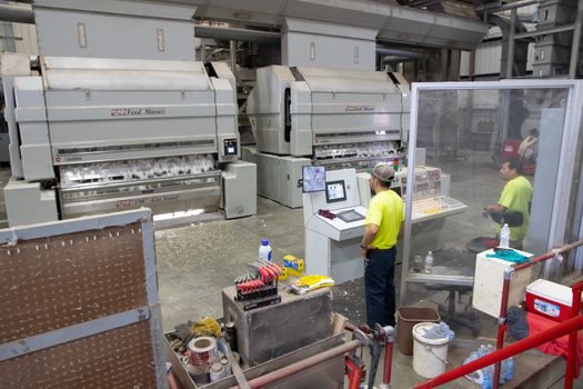
Upgraded metallurgical-grade (UMG) silicon purifies MG-Si through directional solidification, acid leaching, and electron-beam or plasma treatment to remove Fe, Al, Ca, Ti, and P, landing in the 99.999–99.9999% (5N–6N) purity band rather than the 9N+ band of Siemens/FZ electronic-grade product [S3].
UMG-Si is used in commercial multicrystalline solar cells where lifetime tolerance is wider, and in feedstock blends at ≤30% mass fraction with Siemens-grade polysilicon for mono ingot production [S3]. The downstream wafer and cell segment then handles the lower lifetime through gettering and hydrogenation anneals, but UMG never reaches the <1 ppba metal-contamination floor required for IGBT and 300 mm logic wafers — those applications stay on Siemens 9N+ feedstock with optional float-zone refining.
Semiconductor-Grade Refining: Float-Zone and Polysilicon MEMS
Float-zone (FZ) refining passes a molten zone repeatedly along a vertical Siemens rod under RF induction, sweeping metallic impurities to one end of the bar and yielding 99.9999999% (9N+) resistivity silicon for power devices, with resistivities above 10,000 Ω·cm and oxygen below 0.1 ppma [S1]. FZ crystals are pulled directly from the refined rod, so the Siemens CVD step is upstream and FZ acts as a finishing process rather than a standalone route.
The deposition rate, stress gradient, and phosphorus-doping uniformity — typically controlled to ±5% across a 150 mm wafer — define whether the layer can be released without stiction or cracking, and the same reactors also produce polysilicon piezoresistors for pressure-sensor dies linked to industrial pressure transmitter supply chains.
Selection Criteria: Solar-Grade vs Semiconductor-Grade vs MEMS
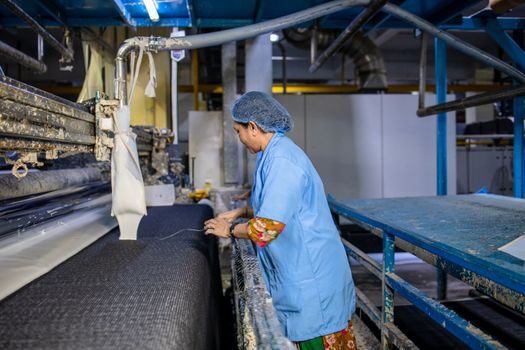
Three decision criteria separate the routes: target purity (6N solar vs 9N+ semiconductor vs MEMS doping tolerance), reactor energy intensity (Siemens 50–70 kWh/kg vs FBR 15–25 kWh/kg vs UMG 5–10 kWh/kg), and downstream form factor (Siemens rod requiring crushing vs FBR granular ready for CZ puller vs UMG chunks needing remelt) [S1][S3].
For solar-grade output at scale, Siemens still owns the installed base, but FBR is the greenfield choice for new mono-wafer capacity because its granular product slots into the same industrial valve and flow meter skids already used in TCS recycle loops; the deciding factor is siting — where cheap hydropower offsets Siemens' high thermal load, FBR's capex premium disappears [S3].
Standards, Process Control and Sourcing Trail
SEMI standards govern polysilicon specification: SEMI MF1398 covers resistivity and carrier lifetime test methods, SEMI MF84 sets trace impurity limits for 9N+ electronic-grade, and SEMI MF1724 defines chunk/granular size distribution for FBR and crushed Siemens feedstock [S3]. Process-side, the polysilicon segment is the upstream input to the solar PV supply chain mapped in the IEA 2022 special report, which traces manufacturing process flow from polysilicon, ingots, wafers, cells and modules, with energy consumption and emissions tracked per kilogram of silicon output [S3].
On the SEC regulatory side, polysilicon producers listing ADSs in New York (e.g. Daqo, Trina Solar historical filings) disclose capacity utilisation rates, ASP per kg, and chlorosilane handling capital expenditure under Item 4 information of their annual 20-F or 424B5 prospectus supplements, with risk-factor language flagging the hazardous-chemistry interface that influences plant siting decisions [S1][S2]. The capital disclosure trail — capacity (t/yr), utilization (%), capex (USD), and ASP (USD/kg) — is the cleanest signal for downstream additive manufacturing material buyers who need to correlate solar-grade silicon surplus with photovoltaic-grade silicon powder entering the powder-bed fusion market.
Failure Modes and Operational Constraints
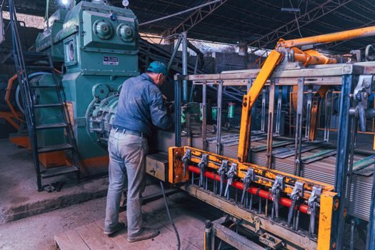
Three recurring failure modes constrain every polysilicon plant: chlorosilane leak and fire, rod breakage inside Siemens bell jars, and fluidization collapse in FBR trains. Siemens bell-jar rod failure is driven by thermal stress during the 1100 °C deposition ramp and typically forces a reactor shutdown every 30–60 batches for rod-string replacement; FBR fluidization collapse is driven by seed-particle agglomeration above 750 °C, which forces operators to throttle silane feed and lose throughput. UMG plants avoid chlorosilane risk entirely but pay a lifetime penalty at the cell that no anneal can fully recover when boron residuals exceed 0.3 ppma. [S1]
On instrumentation, the most failure-sensitive loops are HCl and SiH4 mass-flow control, flow meter drift on the recycle condensate line, and pressure interlocks on the hydrochlorinator; the multifunction process calibrator is the standard field tool for verifying these loops during the annual PSV/flow turn-around that any polysilicon plant above 5,000 t/yr must run to stay compliant with the IEC 61511 safety instrumented system envelope and local ATEX zone classification around the TCS storage pad [S1].
Next node to track: the IEA 2022 special report series' annual update on solar PV manufacturing energy intensity, expected to benchmark 2025 polysilicon energy use per kilogram against the 50–70 kWh/kg Siemens reference and re-rank FBR vs Siemens at the segment level [S3]. A second trackable signal is the SEC 6-K and 20-F cadence of major Chinese polysilicon producers, whose 1H 2026 capacity-utilisation disclosures will set the floor for the next round of solar-grade ASP negotiations.
For related coverage, see Palletizer Price and Cost Guide 2026: Robot, Collaborative and High-Level Tier Map.