Crystalline-silicon photovoltaic cell production runs through a defined seven-stage process flow: polysilicon production, ingot/wafer sawing, surface texturing and cleaning, emitter diffusion, anti-reflection and passivation film deposition, metallization with screen or plating, and final cell/module lamination [S1][S3].
Process support systems — bulk-gas distribution, high-purity chemical delivery, vacuum and exhaust, and slurry recycling — underpin throughput and yield at every one of those nodes, and the white-paper framing of that support layer remains the standard procurement reference for new fab build-out [S1].
Polysilicon, Ingot Growth, and Wafer Preparation
The Siemens-process polysilicon feedstock, typically 6N to 9N purity, feeds Czochralski (CZ) or directional-solidification (DS) mono-like ingot growth; 156 mm and 166 mm M6/M10 wafer formats dominate, with 182 mm M10+ and 210 mm G12 formats scaling into new lines built 2023-2026 [S1][S3].
Wire-saw cutting with diamond-coated brass wire — saw wire diameter trending below 70 μm in 2024-2026 production — defines wafer kerf loss; the related decision between diamond wire and slurry-based cutting is governed by throughput, kerf, and downstream wafer strength rather than by wafer size alone.
Inline metrology at this gate uses resistivity mapping (4-point probe, target 1-3 Ω·cm for p-type CZ) and lifetime measurement (microwave photoconductance decay) to reject sub-prime wafers before they consume chemical and furnace capacity downstream [S1].
Surface Texturing, Cleaning, and Wet Chemistry
Anisotropic alkaline texturing with KOH/IPA (or KOH/texturing-additive blends) on (100) mono-Si produces random-pyramid surface features 3-10 μm in base, dropping front-surface reflectance from ~35% (polished) to below 12% [S1][S3].
RCA-style cleaning — SC1 (NH₄OH/H₂O₂/H₂O) followed by SC2 (HCl/H₂O₂/H₂O) and a final HF dip — strips organics, metals, and native oxide; sequence temperature, bath life, and megasonic-assist energy are the variables that drive queue-time yield on a 100 MW line.
Quartz-tank temperature uniformity within ±0.5 °C and IPA vapour capture at the KOH station are the typical process-engineering gate items at this wet bench; chemical-reclaim units, when fitted, can lift KOH bath life from 24 h to 72 h and are now a default spec on lines above 500 MW annual capacity [S1].
Emitter Diffusion and Junction Formation
P-type emitter formation in n-type cell architectures (TOPCon, HJT, n-PERT) uses POCl₃ liquid-source diffusion in a high-throughput tube furnace at 800-900 °C, with sheet-resistance target 60-120 Ω/sq for front-side emitters and a PSG (phosphosilicate glass) removal step in dilute HF that follows [S3].
Tube-furnace uniformity — defined as ±3-5 °C across the load at peak temperature — is the dominant lever for cell-efficiency spread; a 2 °C peak-temperature shift can move Voc by 4-6 mV on a PERC cell. Atmospheric-pressure CVD, ion-implant, and inline laser-doping alternatives exist but remain minority choices in 2026 mainstream capacity [S3].
Hazardous-gas cabinets for POCl₃, O₂, and NF₃ scrubber sizing (typical 50-200 L/min NaOH wet scrubber) tie the diffusion island into the broader process-support envelope that the fab utility package has to absorb from day one [S1].
Passivation and antireflection (ARC) film deposition are studied in photovoltaic manufacturing process control research, while thin-film solar cell manufacturing requires extensive measurement and control technologies.
Al₂O₃ deposited by plasma-enhanced ALD or PECVD SiNₓ:H stacks form the back-side and front-side passivation/anti-reflection layer; refractive index around 2.05 at 632 nm and thickness ~75 nm are the standard targets for a single-layer SiNₓ ARC on PERC cells [S1][S3].
For TOPCon, a 1-2 nm tunnel-SiO₂ plus 10-20 nm polycrystalline Si stack, grown by LPCVD or PECVD, is the signature layer; plasma-enhanced CVD is the workhorse tool in 2024-2026 capacity because of throughput and gas-cost trade-offs against thermal ALD.
Inline ellipsometer and reflectometer stations monitor ARC thickness to ±2 nm and refractive index to ±0.02 — the same kind of optical process-control discipline documented for ALD/PECVD across adjacent industries such as additive manufacturing material powder-bed runs and multifunction process calibrator loop-checking, where process-gas purity and layer-thickness drift are gated to a known tolerance window.
Metallization, Firing, and Cell Finishing
Front-side Ag paste screen-printed through 280-400 mesh stainless screens, dried at 150-200 °C, and contact-fired in an IR belt furnace at 750-850 °C peak, is the mainstream PERC metallization route. Ag consumption per cell has dropped from ~120 mg (2018) toward 70-80 mg (2025-2026) with multi-busbar and finer-line designs [S1][S3].
Cu-plating on a barrier seed (often Ni/Cu) is the silver-lean alternative; lines configured for plating need additional process-support systems — CuSO₄ chemistry, anode-cathode bus bars, plating-rinse water treatment — that are not in a screen-print fab, and the same kind of utility-coordination discipline shows up in V-process line design and pressure transmitter loop plumbing on chemical-skid build-outs [S1].
Cell-sorting on I-V testers at STC (1000 W/m², AM1.5G, 25 °C) bins finished cells by Pmax, Isc, Voc, and fill factor; typical commercial PERC bins land in the 22.5-23.5% efficiency range in 2025-2026 production, with TOPCon production lines reaching 24-25% in the same period.
Module Assembly: Lay-Up, Lamination, and Framing
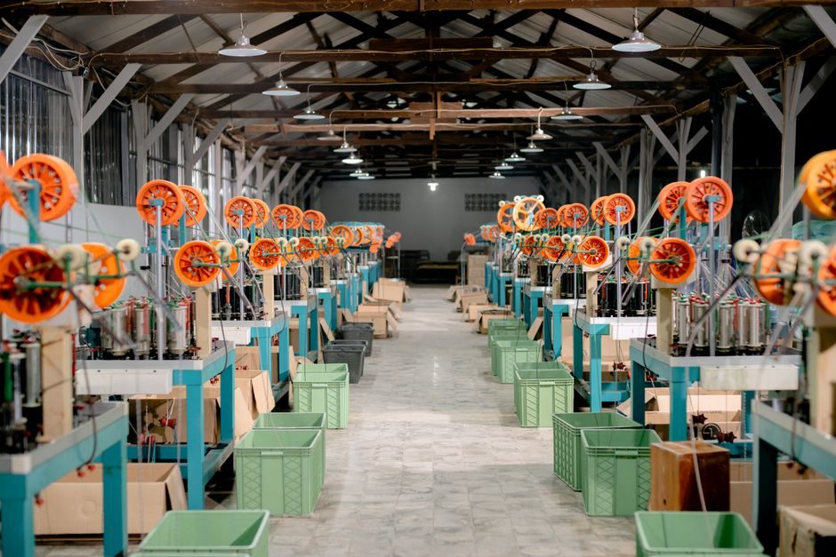
Stringing with copper ribbon (often 0.18-0.25 mm thickness, 1.0-1.6 mm width) tabbed and bus-bar connected, EVA/POE encapsulant lay-up, tempered low-iron glass cover, and a TPT/TPE backsheet are stacked in an automated lay-up station; the lamination press runs 140-160 °C for 12-20 min to crosslink the encapsulant [S1].
Frame options — anodized Al 6005-T5 (common) versus steel-framed utility modules, and frameless glass-glass BIPV variants — change the lay-up tooling and the silicone sealant/butyl edge-seal consumables. Junction-box potting, diode rating (typically 12-15 A Schottky), and IP67/IP68 potted-box certification define the electrical-finish gate before flash-test and Hi-Pot.
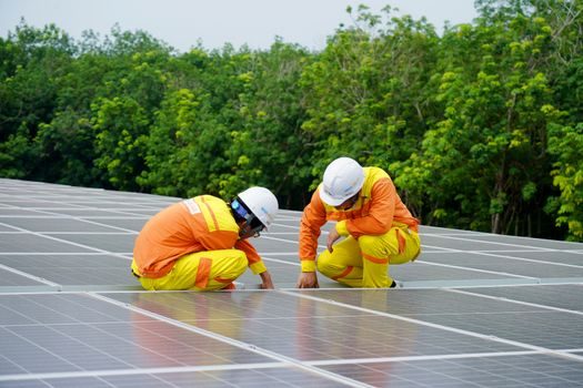
Module-level flash test at STC and electroluminescence imaging close the line; for industrial valve and flow meter work on the same fab utilities, the same source [S1] frames the bulk-gas and high-purity-water support scope that module lines plug into.
Yield, Throughput, and Engineering Trade-Offs
Three trade-off pairs recur in process-engineering reviews: (a) throughput vs conversion-efficiency on metallization — Ag-paste screen-printing wins on throughput, Cu-plating wins on cost/Ag-leverage; (b) furnace diffusion vs ion-implant — furnace is cheaper per wafer, implant is better for selective emitters; (c) wet-chemistry batch vs single-wafer — batch wins on cost-per-wafer, single-wafer tools win on queue-time and data traceability.
For utilities and gas/chemical handling, the framing in [S1] flags bulk-gas (N₂, Ar, O₂, H₂, SiH₄, NH₃), high-purity DI water (typically 15-18 MΩ·cm resistivity), and exhaust treatment (acid scrubber, HEPA, and thermal oxidizer for flammable gases) as the three engineering gates that size the fab utility package.
For a 100 MW to 1 GW fab, build-out lead time from ground-break to first-ingot-pull remains 14-22 months, with tool delivery for diffusion and PECVD the critical-path items; tool-data historian and APC (advanced process control) integration is now a default line-spec rather than a retrofitable option, the same digital-thread pattern called out in chain conveyor and mesh belt conveyor selection guides that sit adjacent to PV fab layout planning.