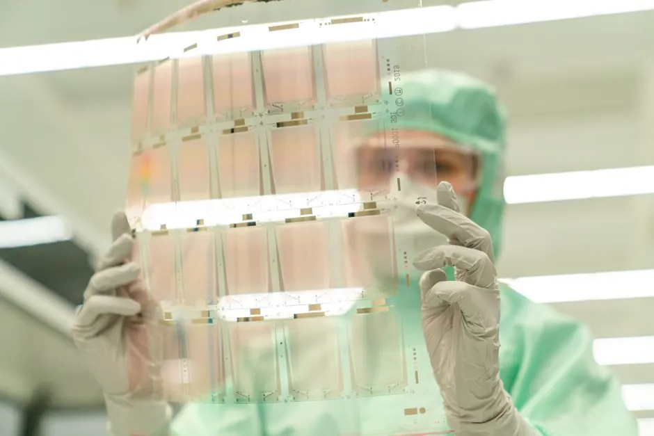
Silicon wafer procurement in 2026 is governed by three orthogonal decisions: a SEMI-standard spec band (SEMI M1 dimension, SEMI MF flat/notch, SEMI M44 resistivity), a merchant-tier sourcing gate (Tier 1 captive IDM, Tier 2 merchant CZ/FZ, Tier 3 reclaim), and a wafer class (Prime, Test, Monitor, Reclaim, SOI or SiC). Global silicon-wafer shipments reached 12,973 million square inches in 2025, up 5.8% year over year on SEMI data, with revenue around USD 11.4 billion [S8].
Bulk silicon-wafer offers on B2B platforms in 2026 sit in a USD 350 to USD 2,500 per piece band on CIF terms, covering Prime, Test, Monitor, SEMI-standard and customized diameters from 2-inch up through 300 mm, plus SOI variants [S4]. The diameter spread itself signals the supplier split: 2" through 100 mm remains standard for MEMS, RF and power-discrete lines, while 150 mm, 200 mm and 300 mm dominate prime-grade semiconductor flows [S4].
Spec Bands Buyers Should Anchor On Before RFQ
Diameter, thickness, crystal orientation, resistivity range, dopant uniformity, surface finish, flatness, and warp are the eight fields that determine whether a wafer survives lithography, deposition, bonding, grinding, and packaging downstream [S3][S6]. SEMI M1 (wafer dimensions), SEMI MF (flat/notch geometry) and SEMI M44 (resistivity) are the procurement language used by every merchant supplier; PCA-style reclaim houses flag SEMI-standard compliance as the baseline for their reclaim output [S4].
For solar mono wafers the conventional form factor is 156 x 156 mm with a ±0.5 mm tolerance, the raw cell form factor used in PV lines; the 2026 supplier map also shows a niche 2-inch diced/amorphous-silicon dice product line at the same suppliers, signalling the specialty-cut end of the merchant market [S4]. Crystal orientation choices (<100>, <111>, custom) and resistivity uniformity are the two fields where OEM device performance is most often lost when sourcing skips the spec review [S5].
Surface roughness, total thickness variation, and warp must meet tight lithography-grade tolerances, and the inspection reports and batch traceability documentation that come back with the lot are part of the spec, not optional paperwork [S5]. Buyers serving power devices, MEMS, sensors, analog products, and R&D lines are the group that gets bitten by ignoring the full spec package, since each downstream step assumes a different slice of those eight fields [S6].
Supplier Tiers and the 2026 Merchant Map
Three tiers are visible in the 2026 supplier set. Tier 1 is the integrated device manufacturers with captive fabs, including Intel, Samsung, TSMC, SK Siltron, GlobalWafers, SUMCO, and Siltronic, that move wafer through long-term agreements and rarely surface on B2B marketplaces [S4]. Tier 2 is the merchant CZ/FZ producers serving external fabs, with the Jiangyin/Songjiang/Shanghai cluster as the most active Chinese node, populated by names like Shanghai Panmeng Electronic Materials and SiBranch Microelectronics in Ningbo, the latter founded 2006 and still active on B2B platforms as of 2026-06-26 [S4].
Tier 3 is reclaim and specialty, and it overlaps with the compound-ceramic supply chain, since the same Chinese merchant hubs list silicon carbide (SiC), silicon-nitride-bonded SiC (SiSiC), reaction-bonded SiC (RBSiC/SiSiC), sintered SiC and recrystallized SiC alongside alumina, zirconia and aluminium-nitride ceramics, material families that double as wafer-handling and furnace furniture [S4]. Buyers sourcing silicon carbide epi substrates or silicon nitride furnace parts from the same merchant cluster should expect cross-quotation overlap with their silicon-wafer RFQ.
India has now appeared on the merchant map as well, with HKTDC's sourcing portal listing Continental Device India Ltd. as a registered silicon-wafer supplier, evidence that the Indian merchant node is visible to global buyers even though Tier 1 capacity remains concentrated in Korea, Japan, Taiwan, Germany, and the United States [S4]. Response-rate data from the Chinese compound-ceramic factories on Alibaba (82.1% and 92.3% in the cited sample) gives a rough handle on merchant-tier responsiveness, with domestic-market and Western Europe as the top shipment corridors [S4].
Prime, Test, Monitor, Reclaim: Choosing the Right Wafer Class
Prime wafers are the unscratched, particle-controlled substrates that go directly into active device fabs. Test and Monitor wafers are used for process-tool qualification and particle or etch-rate monitoring, and go4worldbusiness lists Prime, Test, Monitor, SEMI-standard, and customized as separate SKUs rather than one combined offering [S4]. R&D laboratories typically run a mix, where the procurement goal is to compress material cost without damaging experimental data, so Prime goes into the device wafer, Test into the tool-qualification wafer, and Monitor into the particle/etch-rate wafer [S10].
Reclaim wafers are processed prime wafers recycled back into monitor or test service after polishing and cleaning; the SEMI-standard compliance baseline lets the same supplier serve both prime and reclaim SKUs [S4]. SOI wafers (insulating silicon-dioxide layer with a thin silicon device layer) are a specialized niche for high-performance ICs and need a separate spec conversation on buried-oxide thickness and top-silicon thickness rather than a Prime-style spot buy [S9]. Float-zone (FZ) wafers, with ultra-high purity, high resistivity and low defects, are the standard choice for specialized semiconductor devices and cost more than the equivalent CZ product [S9].
The decision rule that holds across these classes is straightforward: match the wafer class to the process step, not the project budget. Prime on a tool-qualification slot is wasted money, and Monitor on a device wafer is a yield hit, so the spec gate is per process step, not per project [S10].
Documentation, Lead Times, and the Sourcing Gate
Quality documentation on a 2026 wafer lot should include surface condition, dimensional tolerances, packaging, inspection results, and material traceability; the inspection report and the traceability record are how engineering teams verify the wafer will meet the process requirement, and they are also how buyers gain confidence that what is shipped matches what was ordered [S3]. ISO-certified quality systems with in-house testing, statistical process control, contamination monitoring, and documented cleaning processes are the four process-control checkpoints that OEMs are told to look for before signing a long-term agreement [S5].
Lead-time behaviour differs by tier and class: standard SEMI-spec wafers are typically in stock or on a short cycle, while custom specifications (specific resistivity, custom orientation, SOI layer stack, double-side polish) push the schedule out to a custom-engineering cycle that needs explicit planning, not a spot buy [S3][S5]. Buyers running aluminum procurement or UHMWPE lines on the same supplier-visit cadence will see the same merchant-warehouse pattern: standard SKUs ship from local stock, custom SKUs ship from a longer pipeline.
Strong supplier communication is the operational gate that determines whether a custom spec is even feasible: experienced suppliers provide engineering support and fast response on technical questions, and a supplier that cannot do that on a sample inquiry will not do it on a volume order either [S5]. R&D projects need flexible supply because testing often runs through several wafer types before the final process is locked, while production projects need tight consistency, repeatable quality, and reliable supply planning, and the supplier shortlist should be filtered against the stage the project is actually in [S3].
Comparison: Prime vs Test vs Reclaim vs SOI vs FZ

Five wafer classes line up against four decision criteria as follows. On purity and resistivity, FZ is highest (ultra-high purity, high resistivity, low defects), Prime CZ is the mainstream high-quality baseline, Reclaim is reduced from Prime but SEMI-spec compliant, Test and Monitor are typically Prime or Reclaim wafers reused for non-device steps, and SOI is defined by the buried-oxide layer rather than bulk purity [S4][S9][S10]. On cost per wafer in the 2026 B2B band of USD 350 to USD 2,500 per piece on CIF terms, FZ is the highest, Prime is upper-mid, SOI is custom-quoted, Reclaim is the lowest for monitor service, and Test/Monitor sits at or below Reclaim [S4][S9].
On typical use, Prime goes into active device fabs, Test/Monitor into tool qualification and particle/etch-rate monitoring, Reclaim back into monitor or test loops, SOI into high-performance ICs requiring superior isolation, and FZ into specialized semiconductor devices that need the resistivity headroom [S4][S9][S10]. On sourcing complexity, Prime and Test are stock SKUs at major merchants, Reclaim runs through reclaim houses with SEMI-standard compliance, SOI needs a layer-stack spec conversation, and FZ is a specialty product typically quoted per inquiry [S4][S5][S9].
Limits, Failure Modes, and Standards to Watch
The hard limit on the merchant route is Tier 1 capacity. Captive fabs at Intel, Samsung, TSMC, SK Siltron, GlobalWafers, SUMCO, and Siltronic move wafer internally and do not surface on B2B marketplaces, so a merchant-only sourcing strategy caps out at Tier 2 capacity regardless of how good the spec band is [S4]. The other hard limit is application fit: 156 x 156 mm ±0.5 mm mono-PV wafers and the 2-inch diced/amorphous-silicon dice SKU on the same merchant platforms are PV-oriented, with surface quality tuned to PV development rather than semiconductor fab rules, so they fail a Prime device spec even though they pass a price screen [S4].
The recurring failure mode on R&D lines is running a project-budget-driven wafer class across all process steps, which costs the project twice: the device wafer pays Prime prices for monitor service, and the tool-qualification step pays yield when it runs on a wafer that was not engineered for tool-qualification [S10]. Standards discipline matters: SEMI M1, SEMI MF, and SEMI M44 are the procurement language every merchant supplier accepts, and a request for quote that does not reference them signals to the merchant that the buyer is not ready for a serious commercial conversation [S4].
One trackable signal: SEMI's 2025 wafer shipment total of 12,973 million square inches, up 5.8% year over year, sets the volume baseline for 2026 negotiations, and the 2026 B2B offer band of USD 350 to USD 2,500 per piece on CIF terms is the price band the merchant route will actually transact in [S4][S8]. A second signal is the continued visibility of Indian merchant suppliers on HKTDC alongside the Chinese Jiangyin/Songjiang/Shanghai cluster, which gives a multi-region quote option that did not exist as cleanly two years ago [S4].
Spec-level background on the components involved: linear guide.