Silicon wafer manufacturing in 2026 spans monocrystalline Czochralski ingot growth, multi-wire slurry slicing, lapping, single- and double-sided polishing, and final wet or cryogenic cleaning, with wafer diameters of 150 mm, 200 mm and 300 mm dominating semiconductor output and 156 mm / 166 mm / 182 mm formats driving the solar cell line [S3][S6].
Process choice is dictated by end use: semiconductor-grade wafers target sub-nm surface roughness and particle counts below the SEMI-standard adders, while solar-grade wafers (mono- and multi-Si) accept higher saw damage and lower cost per watt, a trade-off that mirrors the broader divergence between silicon carbide power-device substrates and conventional Si production.
Ingot Growth: Czochralski vs Directional Solidification
The Czochralski (CZ) process remains the default route for semiconductor-grade monocrystalline ingots, with hot-zone design, pull speed and seed rotation controlling oxygen and carbon concentration, while multi-crystalline silicon for solar cells is typically produced by directional solidification in quartz crucibles [S3].
Ingot heat treatment — typically 450–900 °C anneals — is used to eliminate thermal donors and repair neutron irradiation damage before wafering, and crystal orientation is verified by X-ray diffraction so that the (100) or (111) lattice plane is referenced for subsequent slicing [S3].
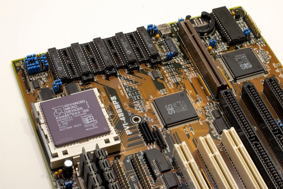
Major Chinese suppliers such as Ferrotec (Ningxia) Semiconductor Technology Co., Ltd. have scaled monocrystalline output to 200 mm and 300 mm class ingots, contributing to China's installed position as a large-volume wafer producer, comparable in capacity-expansion logic to the new aluminum smelting-and-casting lines in Northwest China.
Slicing: From Blade to Multi-Wire Slurry Saw
Wafer cutting has shifted from inner-diameter blade saws to multi-wire slurry sawing, which feeds a single long steel wire through a SiC abrasive slurry and can cut hundreds of wafers in parallel from one ingot, reducing kerf loss versus blade cutting and improving throughput [S3].
Typical solar-grade wafer thicknesses have fallen from ~200 µm in earlier generations to 150–160 µm today, with development tracks pushing toward 120 µm and below, directly lowering the silicon consumption per watt of module output [S1].
Wafer-flatness and thickness-tolerance specs are tighter for 300 mm semiconductor wafers (TTV in the low single-digit µm range) than for solar wafers, a gap that drives much of the equipment selection between slurry saws and fixed-abrasive diamond wire saws, the same kind of spec-versus-cost fork that buyers face when comparing industrial valve classes for chemical versus water service.
Lapping, Edge Grinding, and Damage Removal
After slicing, wafers go through lapping with an Al2O3 or SiC slurry to bring total thickness variation (TTV) under a few µm and to remove the brittle saw-damaged layer, after which edge profiling rounds the periphery to prevent chipping during later handling [S3].
The damaged layer depth removed during lapping and subsequent etching typically runs 10–20 µm per side, leaving a damage-free surface ready for polishing; the same removal-budget logic is used in double-sided polishing of optical glass, where stock removal per side is calibrated against the finished-spec thickness tolerance [S3][S6].
For solar wafers, the lap-and-etch surface is often taken straight to cell processing without the chemical-mechanical polishing step, accepting higher surface microroughness in exchange for lower cost, a deliberate trade-off that line builders re-evaluate each time diamond-wire throughput improves.
Polishing: Single-Sided CMP vs Double-Sided Polishing
Semiconductor wafers are finished on single-sided chemical-mechanical polishing (CMP) tools using colloidal silica slurry, with target surface roughness typically below 0.5 nm Ra and metal contamination controlled at the parts-per-trillion level per SEMI M1 and related standards [S3].
Double-sided polishing is also used for prime wafers and for engineered substrates where both faces need sub-nm finish; this is comparable in concept to the precision-ground stock used in flow-meter orifice plates, where surface finish directly affects measurement bias.
Final cleaning combines RCA-type wet chemistry (SC1 / SC2 with NH4OH-H2O2 and HCl-H2O2) with megasonic-assisted rinsing, and the evolution of cleaning sequences — including dilute HF last-step treatments for native-oxide control — is documented in long-running industry reviews [S5].
Defect Classification: Where Deep Learning Now Sits
Surface-defect inspection has shifted from manual microscopy to automated optical and deep-learning classifiers, with pretrained convolutional networks (ResNet, VGG, Inception variants) benchmarked on wafer defect datasets achieving classification accuracies typically reported in the 90–99% range depending on defect class and dataset balance [S2].
Defect categories tracked on production lines include scratches, particles, pits, edge chipping, micro-cracks, and the "dimple" or "saw mark" defects that correlate with wire-saw wear patterns; in solar lines, these defects directly translate into cell efficiency loss, while in semiconductor lines they translate into die-yield loss [S2][S3].
Inline inspection is typically placed after lapping, after CMP, and after final cleaning, with re-classification feeding back into slicing and polishing tool tuning, a closed loop that has shortened root-cause cycles in modern fabs relative to 2010s-era practice [S2].
Solar Wafer Process Stream: Where Rotameters and Flow Control Sit
Yokogawa's application note on solar silicon-wafer production highlights rotameter use for acid and caustic flow indication in wet-etch and texturing baths, where simple, low-cost local indication is preferred over electronic pressure transmitter loops because the chemistry is well-defined and the lines are short [S1].
The same note frames the dominant cost driver as silicon feedstock and the energy-intensive polysilicon-to-ingot step, not the wafering consumables, which is why throughput per kilogram of polysilicon — not per wafer — is the metric solar-line process engineers watch [S1].
For comparison, similar flow-measurement trade-offs appear in cobalt hydrometallurgy lines, where reagent dosing accuracy and slurry handling dictate the instrument choice more than the absolute flow rate.
Adjacent Substrates: GaN-on-Si and Engineered Wafers
GaN-on-Si engineered wafers — such as those developed by ALLOS for micro-LED display production — add a III-V epitaxial layer on 150 mm or 200 mm Si substrates, allowing LED fabs to reuse Si-line tooling rather than buying dedicated sapphire or SiC lines, a positioning that has accelerated since 2020 [S4].
For power electronics, silicon carbide (SiC) and silicon nitride (Si3N4) substrates address higher voltage and higher thermal-conductivity requirements than silicon can deliver, and the choice between Si, GaN-on-Si, and SiC is now a routine trade-off in inverter and converter design, where the substrate decision drives both the silicon carbide epi-tool spend and the long-term module cost.
Process engineers specifying new wafer-processing lines in 2026 should anchor equipment selection on three numbers: target wafer thickness (µm), TTV budget (µm), and final-surface Ra (nm), with all downstream tool choices — saw, lapper, polisher, cleaner — derived from those three constraints [S3].
The next signal to track is the 200 mm GaN-on-Si roadmap versus the 300 mm Si roadmap through 2027: any acceleration in 200 mm GaN-on-Si epi uniformity will pull more micro-LED and power-device volume off the Si-only line, while continued 300 mm Si throughput gains will keep the cost-per-die gap to SiC wider than the headline SiC growth rate suggests.
For related coverage, see Carton Erecting Machine vs Labeling Machine: Spec Cut for 2026 Pack-Line Buyers.