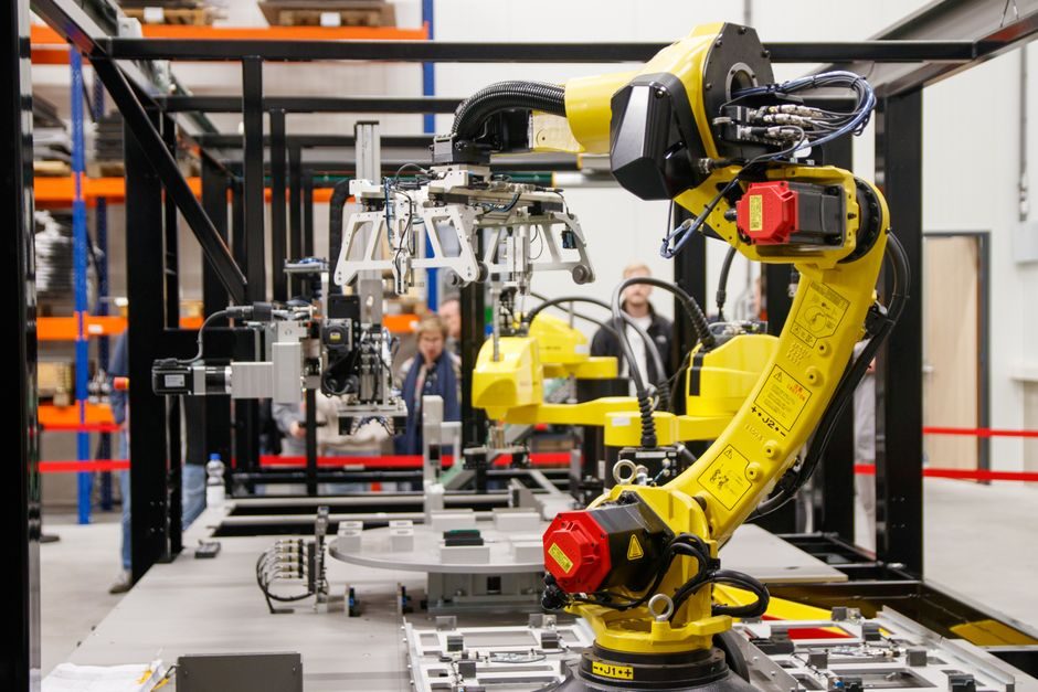
Wafer Fab Equipment (WFE) covers the photolithography, etch, deposition, ion implant, CMP, metrology, wet-clean and test tools that physically pattern and modify silicon wafers in a fab, and the global market is segmented by equipment type, fabrication process stage, node size and end-user per Allied Market Research [S1].
The 2026 WFE supply chain is a three-tier stack: upstream silicon wafer, photomask, photoresist, specialty gas and bulk-chemical suppliers; midstream OEMs including Applied Materials, ASML, Lam Research, Tokyo Electron (TEL), KLA, Hitachi Kokusai Electric, SCREEN and Nikon; and downstream fabs split into foundry, memory, IDM, plus power-device, RF, MEMS, LED and optoelectronics lines per The Business Research Company [S3].
Upstream of every WFE tool sits a narrow base of qualified-material suppliers: 200 mm and 300 mm polished silicon wafers, fused-silica and chrome-on-quartz photomasks, 248 nm / 193 nm / EUV photoresists, electronic-grade gases (NF₃, SF₆, CF₄, Cl₂, HBr, N₂O, SiH₄), ultra-pure water (UPW) and CVD/PVD target materials, all of which are node-qualified by the fab before they ever reach the tool [S6]. Wafer size itself is a market segment — 200 mm, 300 mm and the still-pre-commercial 450 mm class are tracked separately because chamber geometry, handling automation and consumable flows all retool with every wafer-diameter jump [S9].
The OECD 2025 chip-landscape paper flags that extending value-chain data upstream from front-end manufacturing is a stated workstream, because raw-material and gas bottlenecks propagate downstream faster than tooling capacity can be added [S8].
Midstream WFE OEMs: Process Step × Vendor
By process step, the midstream splits cleanly: ASML holds the EUV and immersion-DUV scanner slot, Nikon covers i-line and ArF dry scanners, Applied Materials dominates CVD/PVD deposition and certain CMP platforms, Lam Research owns much of the plasma etch and atomic-layer deposition (ALD) share, Tokyo Electron leads in coater/developer tracks and vertical furnaces, KLA-Tencor runs optical and e-beam inspection and metrology, Hitachi Kokusai Electric in batch furnaces, and SCREEN in single-wafer wet clean [S1][S3].
By node class, the 7 nm-and-below segment is essentially an EUV-scanner-plus-ALD ecosystem; 10–22 nm layers mix ArF immersion with multi-patterning; 32–65 nm is a mature, largely non-EUV, dry-193 nm and i-line production base with strong refurbishment and used-tool trade flows [S1]. Tool classification is two-axis: by fabrication process (front-end-of-line, FEOL, vs back-end-of-line, BEOL) and by functionality (production, R&D, maintenance, quality control), and both axes show up in 2026 WFE market tables [S3].
Downstream Fabs: Foundry, Memory, IDM, Power, MEMS, LED
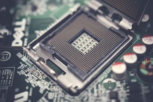
Downstream of the WFE vendor sits the fab floor, and demand is driven by node mix not by unit count: foundry logic (TSMC, Samsung Foundry, Intel Foundry Services, GlobalFoundries, SMIC), DRAM and 3D NAND memory (Samsung, SK hynix, Micron, Kioxia, YMTC) and IDM logic (Intel, Micron-IDM, Texas Instruments, Infineon, STMicroelectronics, Sony Semiconductor) absorb the bulk of the spend, with power discretes, RF GaN/SiGe, MEMS sensors and LED/Micro-LED lines as the long-tail end-users [S3][S9]. Application segmentation in current WFE reports explicitly tracks ICs, MEMS, LED, power devices, RF devices and optoelectronics, and end-use spans consumer electronics, automotive, telecom, industrial and healthcare [S9].
Capacity-add signals read off downstream announcements in 2026 — TSMC's 2 nm Arizona module, Samsung's Pyeongtaek P5, SK hynix's M16 1c-DRAM and YMTC's Wuhan III NAND — drive the WFE order book for EUV scanners, high-current implant, ALD and CMP tools roughly 12–18 months ahead, which is why OEM book-to-bill is the most-watched upstream-to-downstream signal in the chain [S1][S3].
Selection Criteria Buyers Use to Choose a WFE Tool
Selection inside a fab is governed by four non-negotiable filters: process-of-record qualification at the target node, throughput (wph, wafers per hour) at the production recipe, mean wafers between assists (MWBA) and mean time between failures (MTBF) for cost-of-ownership, and roadmap alignment with the OEM's next-node platform — qualification is binary, throughput is linear, and MWBA is the dominant CoO lever past 28 nm [S7].
On top of those, fabs segregate by wafer size: 200 mm lines for analogue, power, MEMS and mature-node logic; 300 mm lines for sub-28 nm logic and advanced memory; 450 mm remains a future option with no high-volume fabs shipping product in 2026, so the operational decision is between buying a new 300 mm tool, buying a refurbished 200 mm tool, or extending a tool's life via upgrades and OEM service contracts [S9].
Material & Process Constraints Across the Chain
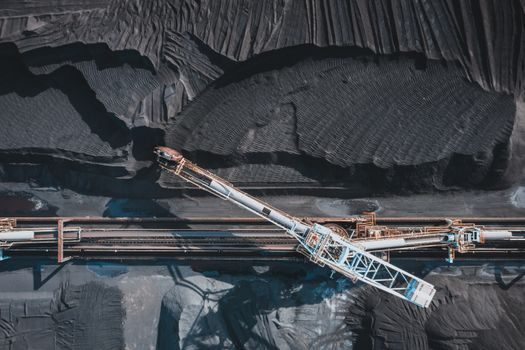
Three constraints bind the chain end-to-end. Raw-material specificity is a gating concern, and Allied Market Research lists the requirement of very specific raw materials as a structural restraint on the wafer fab equipment market [S1]. Second, state-of-the-art machinery capex: a single EUV scanner list price is publicly discussed in the ~US$200M band, and a 300 mm fab module runs several billion US dollars, which is why foundry, memory and IDM dominate the end-user table rather than smaller fabless or fab-lite players [S1].
Third, technology compatibility: lithography wavelength, photoresist platform and hardmask stack must be qualified as a set — 193 nm immersion with chemically amplified resist is a different tool-and-consumable pair than EUV with metal-oxide resist, and mixing across generations is a process-engineering fault, not a configuration option [S3]. Process-engineers reading a WFE bill-of-materials treat the tool, the chemistry, the mask and the metrology as a single coupled system [S7].
Comparison of WFE Options by Decision Criteria
Side-by-side, the three dominant process-step categories diverge sharply on the criteria a process engineer actually picks on. Photolithography tools (ASML EUV/DUV, Nikon) score highest on node roadmap and lowest on throughput-per-dollar at the 7 nm-and-below node; deposition tools (Applied Materials CVD/PVD/ALD, Lam ALD) score highest on film-uniformity and CoO per wafer; etch tools (Lam, TEL) score highest on selectivity and aspect-ratio at 3D NAND and DRAM stair-stack steps; metrology/inspection (KLA, Hitachi) scores highest on defect sensitivity but is non-value-add in throughput terms [S1][S3].
For a 200 mm vs 300 mm decision the comparison is simpler: 200 mm wins on tool price, refurbished availability and suitability for power/MEMS/analogue, while 300 mm wins on die-per-wafer economics, automation maturity and advanced-node access — and 450 mm currently has no commercial line shipping in 2026, so the practical fork is between 200 mm brownfield and 300 mm greenfield [S9].
Use Cases, Limits, and Failure Modes
The cleanest use-case splits are by end-user. Foundry lines buy for logic node migration, memory lines buy for stack-height and bit-density scaling (3D NAND layer count, DRAM 1a/1b/1c/1d nodes), IDM lines buy for in-house product cycles, and power/RF/LED lines buy for cost-per-die at mature nodes on long tool lifecycles [S3][S9]. Equipment is therefore specified by the fab's end-product roadmap, not by the OEM's flagship product.
Limits and failure modes are concentrated at three points: chamber-parts wear (quartz, ESC, showerhead, O-rings) drives unplanned downtime; gas-delivery and abatement line fouling forces preventive maintenance intervals; and upstream raw-material contamination (a single lot of off-spec photoresist or gas) can scrap a full wafer batch before metrology even flags it [S7]. The OECD value-chain note explicitly warns that upstream data extension is needed precisely because these raw-material and gas shocks propagate downstream faster than tooling capacity can be added [S8].
Standards, Sources, and Trackable Signals
No single IEC or ISO standard governs WFE as a system; instead the chain is anchored in SEMI standards (SEMI E10 for yield management, SEMI E84 for carrier-handling, SEMI E87 for CIM framework, and SEMI E93 for SECS-II/HSMS messaging) plus the relevant ITRS/IRDS node roadmaps, with fabs holding their own process-of-record qualification on top of any compliance layer [S7][S10]. Sourcing maps cross-reference the same WFE market by node size (7 nm-and-below through 65 nm-and-above), fabrication process (FEOL vs BEOL), end-user (foundry, memory, IDM) and region (North America, Europe, Asia-Pacific, LAMEA) [S1].
Two trackable signals for the next quarter: the Q3 2026 WFE order intake at ASML, Applied Materials, Lam Research, TEL and KLA, and the 200 mm vs 300 mm capex split in the TSMC, Samsung, SK hynix and Micron capex updates for FY 2026. For spec-driven comparison context, a current lithography-equipment supplier map reads well against the photolithography segment above, while a wider NAND flash supply and capacity view ties directly to the memory down-stream bucket.
Component reference pages worth checking: anti static equipment, pressure transmitter, and flow meter.