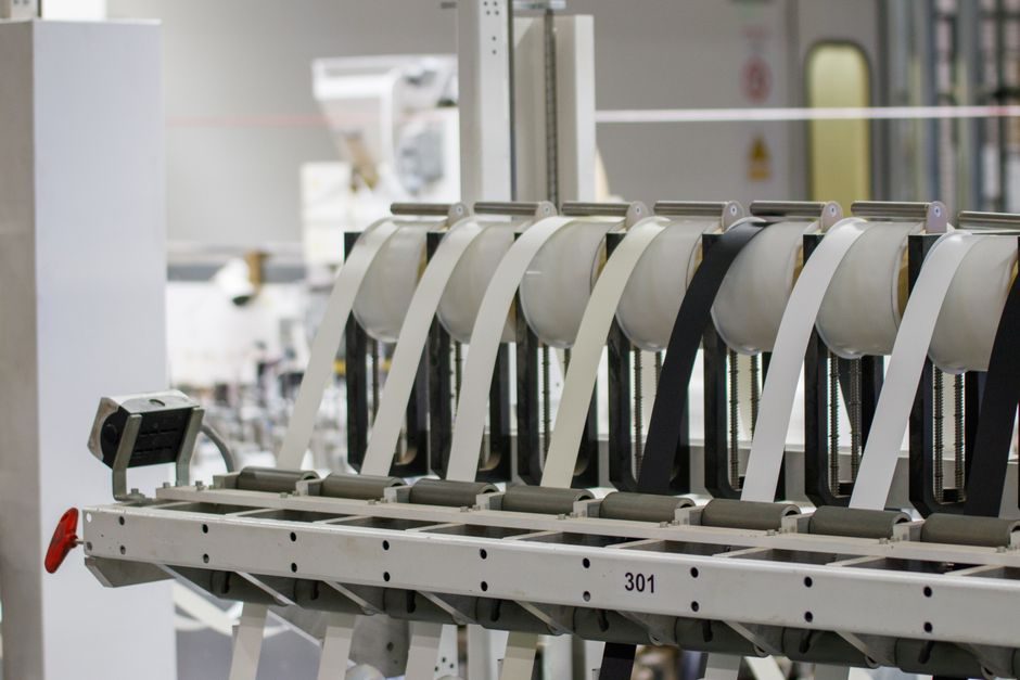
ASML is the sole supplier of production EUV systems, while Canon and Nikon split the ArF immersion/KrF/i-line installed base, and Leica, Raith, SUSS MicroTec, JC Nabity, NIL Technology, Nanonics, Nanoink and Rolith cover the nanolithography and research tool segment [S2][S3].
Buyers looking at the lithography equipment market in 2026 should treat the supply base as a three-tier pyramid: EUV at the apex (single supplier, 13.5 nm-class production), ArF immersion/KrF/i-line in the middle (three main OEMs, deep second-hand availability), and nanolithography/EBL/research tools at the base (multi-vendor, fragmented) [S2]. The broader market was US$22.1 Bn in 2022 and is forecast to reach US$41.3 Bn by 2031 at a 7.2% CAGR [S7].
Three-Tier Manufacturer Map: EUV, ArF/KrF/i-line, and Nanolithography
The 2018–2023 nanolithography equipment market study lists ten manufacturers across the segment: ASML, Canon, Leica, Raith, SUSS MicroTec, Rolith, Nanoink, Optical Associates, Nanonics Imaging, JC Nabity Lithography Systems, and NIL Technology [S2]. That list still maps cleanly onto the 2026 supplier base because EUV remains an ASML monopoly and ArF/KrF/i-line are still split between ASML, Nikon, and Canon.
Lithographic equipment is the single most expensive step in wafer fab, used to print complex circuit patterns onto silicon wafers that are the primary raw material for integrated circuits [S2]. For process engineers, that means the supplier list is short at the top, and OEM selection drives 5–10-year service contracts, not just unit price.
Decision Criteria: Wavelength, Resolution, Application, and Service Geography
Lithography tools split first by exposure wavelength — ArF Dry, ArF Immersion, KrF, EUV, and i-line — and second by application: foundry, memory, or IDM [S2]. EUV is the only option below roughly 7 nm logic half-pitch in production today, ArF immersion with multi-patterning still handles 7–28 nm, and KrF/i-line remain workhorses for non-critical layers and mature nodes.
The GlobalSpec supplier index alone lists 64 lithography equipment suppliers against a 106,438-manufacturer and 20,791-distributor global catalog, with 62,441 manufacturers headquartered in the United States and 43,997 headquartered outside it [S1]. That imbalance tells you the distribution and service channel is global, but the IP and OEM headquarters cluster in the US, Netherlands (ASML), Japan (Canon, Nikon), and Germany (SUSS, Raith, Leica heritage).
Comparison of Main Lithography Tool Types on Engineering Criteria
On four decision criteria — minimum resolution, capital cost, throughput, and application fit — EUV (ASML NXE:3800E class) leads on resolution at roughly 13 nm half-pitch and sub-100 W source power per layer, but at the highest capital cost and tightest service footprint. ArF immersion sits in the 38–32 nm single-exposure range, scales via double/triple/quadruple patterning down to ~7 nm, and costs roughly a third of an EUV tool. KrF and i-line handle non-critical layers (back-end metal, passivation, pad) at the lowest cost per wafer, and nanolithography/EBL (Raith, JC Nabity, Leica heritage) targets sub-100 nm R&D work at low throughput [S2][S3].
Buyers should match tool type to layer criticality, not chase the smallest wavelength: a memory fab running 1z/1α DRAM still runs mostly ArF immersion and KrF, and only pulls EUV for one or two critical layers. For sensor-heavy process lines that already spec pressure transmitters and flow meters for upstream gas/chemical delivery, the lithography tool choice cascades back into the industrial valve and PLC spec for the make-up gas and immersion water loops.
Use Cases: Foundry vs Memory vs IDM vs Research
Application split is foundry, memory, and IDM [S2]. Foundry customers (TSMC, Samsung Foundry, Intel Foundry Services) drive EUV adoption because their customer mix is logic-heavy and node-aggressive; memory customers (DRAM, NAND) absorb EUV more selectively, typically 1–2 layers per die; IDM fabs in automotive, MEMS, and analog still run mostly ArF/KrF/i-line, often on tools 10+ years old.
For university, government, and pilot-line R&D, the supplier set is Raith (EBL and focused ion beam), SUSS MicroTec (mask aligner, nanoimprint), Leica heritage tools (EBL adapted from SEM/STEM columns), JC Nabity (low-cost EBL retrofit), NIL Technology (nanoimprint lithography, NIL), and Nanonics Imaging (near-field, AFM-correlated lithography) [S2][S3]. The 1994 Leica Cambridge paper showed the core EBL component technology was already scaling from the 100–10 nm into the 10–1 nm range using STEM/SEM column technology [S3] — a baseline the commercial vendors still build on.
Limitations, Failure Modes, and Sourcing Risks
Single-supplier risk on EUV is the dominant constraint: no second source exists, and lead time on a new EUV system is typically 12–18 months. For ArF/KrF/i-line, the constraint shifts to service continuity — Canon and Nikon both have large installed bases but differ in field-service coverage outside Japan and the EU. For nanolithography/EBL research tools, the constraint is application fit (beam current, stage accuracy, stitching, overlay) rather than capital cost; adapted SEM/STEM columns can hit sub-10 nm spot size but lack integrated nano-positioning and overlay metrology for production-style work [S3].
Sourcing also has to plan for ancillary equipment. A complete lithography cell pulls anti-static equipment for wafer/reticle handling, pressure sensors on the immersion water and gas cabinets, and a controls stack that the fab PLC has to sequence against the exposure tool handshake. For the full cost stack, the supply-chain deep-dive is in Lithography Equipment Supply Chain 2026, and the upstream/downstream module map is in Lithography Equipment Upstream and Downstream Map.
Standards, Sourcing Channels, and Verifiable Next Signals
Lithography equipment sits outside the ATEX/IECEx pressure-equipment scope, but the gas-delivery and chemical-delivery skids around it do, so fab buyers typically cross-reference the same ISO/IEC quality and safety frameworks used for pressure transmitters and flow meters. For sourcing channel data, GlobalSpec maintains a searchable lithography equipment manufacturers and suppliers page [S1], and a lithography equipment market outlook reports the market at US$22.1 Bn in 2022, projected to reach US$41.3 Bn by 2031 at a 7.2% CAGR [S7].
Trackable signals over the next two quarters: new EUV tool shipment announcements from ASML (capacity constraint indicator), Nikon/Canon ArF immersion tool order books (memory capex proxy), and nanolithography vendor M&A (Raith, SUSS MicroTec, NIL Technology consolidation is the most likely shape). For sister-fab context on industrial valves and PLC selection that has to match the lithography tool's utility specs, the Specialty Chemicals Smart Manufacturing spec roundup is the cleanest cross-reference.