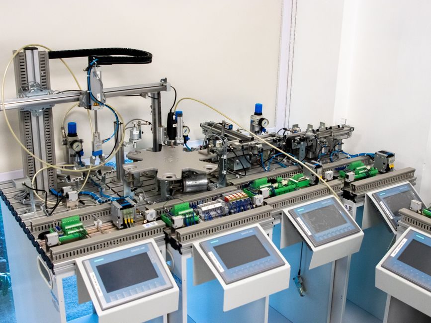
AI accelerator silicon — edge TPUs, industrial GPUs, and inference SoCs — has become the single largest capex line item inside Industry 4.0 (I4.0) retrofit budgets, reshaping how foundries, casting lines, and discrete-parts plants sequence their digital transformations [S2].
What changed between 2024 and mid-2026 is the locus of compute: inference workloads that used to require a centralized server rack are now specified at the cell or station level, driven by AI/ML metamodels that demand sub-100 ms closed-loop response for property control in processes such as ductile iron sand casting [S6]. For a process engineer, the practical question is no longer whether to adopt I4.0, but which silicon tier — edge inference, industrial GPU, or hyperscale-class accelerator — pairs with which control loop.
Where AI Chips Sit Inside the I4.0 Stack
AI silicon is now specified at three distinct layers of the I4.0 reference model: the edge (cell-level inference on PLC or industrial-PC form factors), the fog (line-level aggregation), and the cloud (training and fleet-level optimization) [S2]. Edge inference chips handle time-critical loops — for example, pouring temperature and cooling-rate compensation in sand casting — where round-trip latency above ~50 ms degrades closed-loop performance, while training workloads remain on industrial-GPU or data-center accelerators [S6].
The split mirrors the foundational technology taxonomy: cyber-physical systems (CPS), the Industrial Internet of Things (IIoT), big-data analytics, cloud computing, augmented reality, autonomous robots, additive manufacturing, and AI itself [S2]. Each tier pulls a different silicon footprint, and procurement teams are now expected to match chip TDP, memory bandwidth, and industrial certifications (IEC 60079-x for hazardous-area edge nodes, where applicable) to the physical layer above the flow meter or pressure transmitter feeding the loop.
Adoption Maturity by Technology and Region
Structured literature reviews classify I4.0 technologies along six adoption stages — intention, adoption, implementation, routinization, continuance, and diffusion — and the 2022 maturity analysis placed AI/ML and IIoT at the implementation-to-routinization frontier, behind cloud computing but ahead of blockchain and many AR use cases [S4]. In practice, that means 2026 deployments are scaling routinized IIoT sensor layers while AI/ML is still moving from pilot to production in most SMEs.
Regional maturity diverges sharply. An ISM study of Indian SMEs ranked cost of investment, cybersecurity risk, and lack of skilled workforce as the top three dependency-level barriers to I4.0 adoption, with smaller firms disproportionately blocked at the intention stage [S1]. Brazilian manufacturing data from 135 firms found that organizational-learning capabilities mediate the link between I4.0 technology adoption and operational performance, with learning maturity explaining a meaningful share of variance in scrap and throughput outcomes [S3]. A separate 2024 study of high-performance ductile iron sand casting showed that AI/ML-driven metamodels can simultaneously target multiple design objectives — tensile strength, elongation, hardness — once enough labelled process data is available [S6].
AI Chip Selection Criteria for Industrial Loops
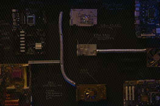
Procurement engineers in 2026 are evaluating edge AI silicon against four criteria: latency budget, operating-temperature range, hazardous-area certification, and software-toolchain support for industrial protocols. Edge inference SoCs targeting cell-level loops typically need sub-50 ms inference at 1–10 W, while line-level aggregation nodes run industrial GPUs in the 75–300 W range with ECC memory and conformal-coated PCBs [S2].
A simplified comparison of the three dominant silicon tiers for I4.0 retrofits:
• Edge inference SoC (e.g. TPU-class NPU, Jetson-class modules): power 5–30 W, latency 10–50 ms per inference, best fit for station-level closed-loop control adjacent to a PLC; hazardous-area variants require IEC 60079-x or ATEX 2014/34/EU certification.
• Industrial GPU node (T4/L4 class, Xeon-class CPUs): power 75–300 W, latency suitable for batch inference and vision QA, deployed in control-room cabinets.
• Hyperscale accelerator (H100/MI300 class): power 700+ W, reserved for offline training and fleet-level digital-twin simulation, not deployed on the plant floor.
For foundries running ductile iron sand casting, the documented AI/ML framework uses real-time process data from pour temperature, cooling rate, and inoculant chemistry to predict as-cast tensile and elongation, then feeds corrections back to the line [S6]. That loop only stays closed if the inference node sits within ~5 m of the sensor cluster — a layout constraint that often dictates chip selection over raw TOPS ratings.
Who Benefits and Who Is Locked Out
Plants that already operate routinized IIoT sensor networks — typically large OEMs and Tier-1 suppliers with multi-year digital roadmaps — are extracting measurable scrap and energy savings from AI-chip retrofits [S3][S4]. The Brazilian empirical study showed operational-performance gains concentrated in firms with higher organizational-learning maturity, meaning the same silicon produces very different results depending on the workforce's ability to interpret model outputs and override them safely [S3].
SMEs, by contrast, remain gated by the same barriers documented in the Indian ISM analysis: capital cost, cybersecurity exposure, and a thin bench of data engineers and process-control specialists [S1]. A 2024 supply-chain-financing study confirmed that SME cash-flow constraints and weak digital infrastructure remain the binding constraints on I4.0 tool adoption, even when financing windows are open [S5]. Plants without continuous data historians, calibrated pressure sensor networks, or standardized tag naming should not buy AI silicon first — the chip will sit idle waiting for data the plant cannot produce [S2].
Failure Modes and Cybersecurity Constraints
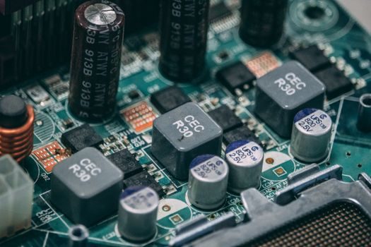
The dominant failure mode in 2025–2026 I4.0 retrofits is not the AI model but the data pipeline feeding it. Drift in sensor calibration, time-sync loss between edge nodes, and adversarial input on machine-vision streams have all been flagged in the foundational literature as structural risks of hyperconnected I4.0 systems [S2]. Edge AI chips do not solve these — they amplify the consequences by acting on bad data faster than a human operator can intervene.
Cybersecurity is therefore the gating constraint, not an afterthought. ENISA and the academic literature both identify hyperconnectivity as the primary attack-surface expansion of I4.0, and recommend network segmentation between IT and OT layers, hardware-rooted trust on edge nodes, and continuous monitoring of firmware integrity [S2]. For plants deploying AI accelerators in hazardous areas, certification paths under ATEX 2014/34/EU and IEC 60079-x for explosive atmospheres still apply, and the chip vendor's willingness to support those certification cycles has become a tie-breaker in RFQs.
Standards and Sourcing Discipline
Engineers specifying AI silicon for I4.0 should anchor procurement to the established standards stack: IEC 61131-3 for PLC programming, IEC 62541 (OPC UA) for interoperability, ISO 9001 and IATF 16949 for quality systems, and ATEX 2014/34/EU or IECEx for hazardous-area deployment. ISO/IEC 23053 for AI systems using a machine-learning approach provides a framework reference for the model side, though it is not a safety standard [S2].
Buyers should demand from vendors: published TOPS at a stated precision (INT8 vs FP16), operating-temperature range with derating curves, mean-time-between-failure (MTBF) figures, hazardous-area certificate numbers where applicable, and a software bill of materials (SBOM) for the inference stack. Plants that already have a routinized IIoT layer — the maturity stage identified in the 2022 adoption review [S4] — are the realistic near-term buyers; everyone else is buying a science project.
For an engineer mapping a 2026 retrofit, the trackable signal is fab capacity: foundry expansion for sub-7 nm AI accelerator tiles and advanced packaging (CoWoS, SoIC) will gate edge-class supply through 2027, so locking in allocation now matters more than squeezing 10% off unit price.
Related analysis: Lost Foam Casting Line Installation: Zone Map, Acceptance Specs, and Pitfalls.