
The global AI chip market is forecast to grow by USD 154.93 billion over 2025–2030 at a 24.3% CAGR, with North America holding the largest share and the ASICs segment sized at USD 16.70 billion in 2024 [S7]. This is the most actionable single number for any process engineer or sourcing manager building an AI-related BOM right now.
Put against the wider market, the AI market (chips + software + services) is valued at USD 601.93 billion in 2026 and is projected to reach USD 3,638.08 billion by 2033 at a 29.3% CAGR, per MarketsandMarkets [S8]. Next Move Strategy Consulting tracks a narrower slice: AI market value of USD 224.41 billion in 2024 growing to USD 1,236.47 billion by 2030 at 32.9% CAGR [S1]. The two reports bracket the same direction with different scopes; both are useful for sanity-checking procurement volume assumptions.
Hardware segment: chips, memory, storage inside the AI stack
Within the AI market, the hardware offer segment — AI chips, memory, and storage — sits alongside software and services in MarketsandMarkets’ 2026–2033 forecast, with the total AI market reaching USD 3,638.08 billion by 2033 at 29.3% CAGR [S8]. Technavio’s narrower AI chip line item is the one that matters for foundries, OSATs, and substrate suppliers: USD 154.93 B incremental opportunity, 24.3% CAGR, 2025–2030 [S7].
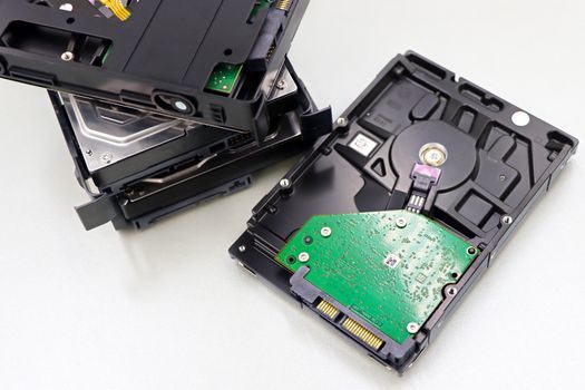
Inside that chips-only pool, ASICs alone were a USD 16.70 billion segment in 2024 and dominate the discussion because they let hyperscalers and OEMs tune silicon for specific inference and training workloads [S7]. For the industrial control buyer, this matters even if you never order a GPU: the same foundries and packaging lines feed the PLC and pressure transmitter supply chain, so wafer and substrate lead times are now coupled to AI demand.
Architecture split: GPU, ASIC, and the Chinese three-track divergence
GPU architecture has been the mainstream AI compute baseline, with NVIDIA’s CUDA ecosystem building a hard-to-displace moat [S9]. On 2026-05-17, Smart Compute Chip World published the “2026 China AI Compute Chip Market Research Report,” which describes three differentiated Chinese architectural tracks rather than a copy-NVIDIA path: Huawei’s Da Vinci (full-stack in-house, positioned as the domestic performance benchmark), plus two other in-house tracks aimed at inference and edge workloads [S9].
For buyers, the structural takeaway is a three-way race — general-purpose GPU (NVIDIA-class), hyperscaler ASIC (Google TPU, Amazon Trainium/Inferentia, Microsoft Maia lineage), and the emerging Chinese full-stack track — and each of them has a different bill of materials, packaging profile, and HBM memory ratio. The same supply tension shows up downstream in adjacent categories covered in our semiconductor industry trends 2026 brief, where test capacity and advanced packaging (CoWoS, 2.5D/3D) are the binding constraints.
Geography: North America leads, China builds parallel stack
North America dominated the AI chip market in Technavio’s 2024 snapshot and accounts for the majority of incremental dollars through 2030 [S7]. That concentration is reinforced by where the leading fabless designers, EDA vendors, and large-language-model training clusters are physically located.
China’s response, per the 2026-05-17 Sina-hosted report, is a three-track domestic architecture strategy — Huawei Da Vinci, plus two parallel in-house lines — explicitly framed as moving from “follow” to “original creation” rather than re-implementing CUDA [S9]. For a sourcing manager this is a two-supplier-region world by 2026: North American/ Taiwanese-Korean design + foundry for the leading edge, and a Chinese stack serving domestic hyperscalers and select export markets. The industrial valve and flow meter supply chains are not AI chips, but they sit in the same fabs and substrate houses, which is why their lead times now move with AI build-outs.
Options matrix: GPU vs ASIC vs custom Chinese stack
For a buyer or process engineer trying to place a bet, the three options line up against four criteria: [S1]
<b>Performance per watt for training.</b> General-purpose GPU (NVIDIA H100/B100 class) still leads on raw training throughput and software maturity (CUDA) [S9]. Hyperscaler ASICs trail on raw FLOPs but close the gap on perf/W for their target workloads; domestic Chinese Da Vinci-class parts are positioned as the domestic perf benchmark but are still building an independent software stack [S9].
<b>Ecosystem and toolchain lock-in.</b> GPU/CUDA wins on day-one productivity; ASIC requires in-house compiler work but pays back at scale; Chinese stacks require porting effort and accept the ecosystem risk in exchange for supply security [S9].
<b>Supply and lead time.</b> GPU supply is gated by CoWoS advanced-packaging capacity at TSMC; ASICs share that bottleneck but lock in long-term wafer agreements; Chinese stacks route to SMIC and local OSATs, which have their own capacity ceiling [S7][S9].
<b>Unit cost at volume.</b> GPU carries the highest per-device ASP; ASIC wins on cost-per-inference at hyperscaler scale; domestic Chinese silicon is competitive on domestic-currency cost for the Chinese market segment [S7][S9]. Across all three, the binding production constraint is advanced packaging and HBM memory, not raw wafer count.
Adjacent signals: how AI demand ripples into industrial electronics
The AI chip cycle is the new top-of-stack driver for the same fabs, substrates, and OSAT lines that serve industrial buyers. Technavio’s USD 154.93 B incremental pool at 24.3% CAGR is large enough to redirect advanced-node capacity away from non-AI lines for the next 24–36 months [S7]. That crowding shows up indirectly in the semiconductor industry trends 2026: talent, test, and packaging shifts — test cells, CoWoS-equivalent capacity, and HBM stacking are the choke points.
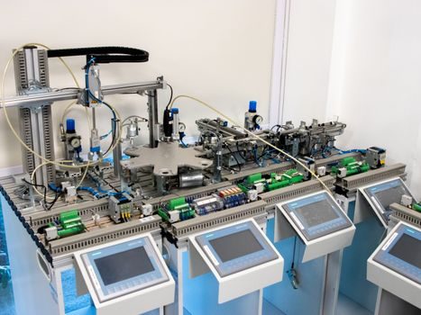
For the industrial buyer the practical effect is longer lead times and rising ASPs on pressure sensor modules, PLC CPUs, and servo drive MCUs that share mature-node fabs with AI-adjacent silicon. Sourcing teams should plan for 30–40-week lead times on advanced-packaging-dependent parts through 2026 and qualify second sources now.
Sourcing standards and verifiable next nodes
No single IEC, ISO, JEDEC, or SEMI standard fixes the AI chip market size — the figures here are market-research outputs, not regulatory ones. Use the three cited forecasts as a triangulation set, not a single source of truth: Technavio for chips-only incremental dollars (USD 154.93 B, 24.3% CAGR, 2025–2030), MarketsandMarkets for the full AI market stack (USD 601.93 B in 2026, USD 3,638.08 B by 2033, 29.3% CAGR), and Next Move Strategy Consulting for the AI market perimeter (USD 224.41 B in 2024, USD 1,236.47 B by 2030, 32.9% CAGR) [S7][S8][S1].
Track these three signals over the next two quarters to confirm or refute the trajectory: (1) CoWoS and HBM stacking capacity expansion announcements from TSMC and SK hynix, (2) hyperscaler ASIC volume disclosures (TPU v6/v7, Trainium 3, Maia 2 lineage), and (3) follow-on releases of Chinese Da Vinci-class roadmaps from Huawei and adjacent domestic vendors [S9]. The 2026-05-17 report is the most recent China-specific architecture roadmap in this dataset; the next credible checkpoint is Q3 2026 OEM earnings calls, which will disclose real shipment volumes against the 24.3% CAGR trajectory [S7][S9].