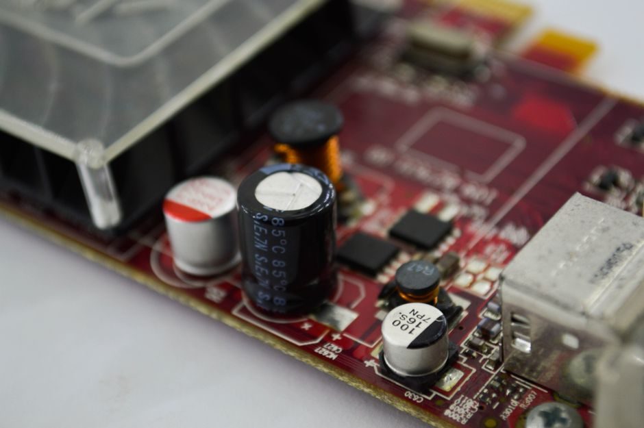
For AI accelerators, OEM and ODM are no longer abstract commercial terms — they map directly onto foundry process ownership, CoWoS-S/L advanced-packaging allocation, and HBM3e/HBM4 stack sourcing, with the OEM path typically carrying higher NRE but tighter IP control, and the ODM path cutting tape-out lead time by leveraging a pre-validated reference design [S4][S9].
The decision sits on top of three physical chokepoints documented across the 2026 supply chain: advanced-node wafer capacity at ~3 nm/2 nm, CoWoS interposer throughput, and qualified HBM stack supply — see the breakdown in AI chip manufacturing cost breakdown: 2026 wafer, packaging, and HBM drivers. Buyers picking the wrong path here get hit twice: once on NRE amortisation, once on missed production windows.
Definition Split: OEM Contract Build vs ODM Reference Design
OEM (Original Equipment Manufacturer) means the factory produces to the buyer's complete, buyer-owned specification — the buyer owns the RTL, the GDSII, the mask set, and the validation plan, and the foundry executes. In the AI accelerator world this is the Nvidia/Ampere/Graphcore-style model where the foundry (TSMC, Samsung) and OSAT (ASE, Amkor) are paid per wafer and per package for a build that the customer has fully architected [S4].
ODM (Original Design Manufacturer) means the manufacturer has already produced a working reference design — RTL, firmware, board, and sometimes chassis — and the buyer rebrands it or requests light modification. The contract is for a near-finished product, not a blank wafer [S9]. In AI silicon this shows up as merchant accelerator IP houses shipping hard-macro chiplets, or as white-box server ODMs (Quanta, Wiwynn, Inventec, Foxconn) taking a reference accelerator module and integrating it into a rack with their own BMC, PLC management plane, and chassis.
Decision Criteria: NRE, Time-to-Tape-Out, IP Control, Packaging Access
Four engineering criteria separate the paths cleanly. NRE: an OEM tape-out at 3 nm including mask, IP licensing, and bring-up routinely runs an order of magnitude above an ODM reference-design licence fee, which is why only well-funded buyers sit on the OEM side of the leading edge [S4]. Time-to-tape-out: ODM cuts 6–12 months off the schedule because the RTL is pre-verified on a reference platform — the cost is that differentiation must come from software, memory hierarchy tuning, or system-level flow meter of data, not from a novel core [S9].
IP control: OEM gives the buyer full RTL/SoC ownership and freedom to file patents around microarchitecture; ODM typically constrains the buyer to brand and software differentiation, with the silicon IP held by the design house. Packaging access: OEM buyers can directly secure CoWoS-S or CoWoS-L interposer capacity and HBM3e/HBM4 stack allocation; ODM accelerator buyers inherit whatever packaging the reference design was qualified on, which constrains memory bandwidth and TDP headroom — see AI Accelerator Supply Shortage 2026: Eight Categories Tight, No Drawdown Mechanism.
Criteria Matrix: OEM vs ODM on AI Chip Procurement
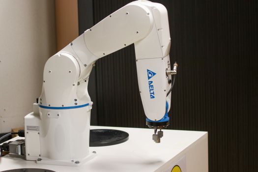
Lining the two paths against the criteria above: NRE cost — OEM high (mask + IP licence + bring-up), ODM low (reference-design licence or per-unit royalty). Time-to-production — OEM slow (12–18 months typical tape-out cycle), ODM fast (3–6 months to a working rack). IP ownership — OEM full, ODM limited to software/system layer. Packaging control — OEM direct allocation of CoWoS/HBM, ODM inherits reference design's qualified BOM. Differentiation ceiling — OEM unrestricted (core, fabric, memory topology), ODM bounded (firmware, topology, system pressure sensor telemetry) [S4][S9].
For hyperscaler-class buyers with proprietary model architectures, the matrix points firmly to OEM — the differentiation ceiling is where AI accelerator value is created, and the NRE is amortised across hundreds of thousands of units. For enterprise buyers, tier-2 cloud providers, and edge-AI integrators, ODM wins on cost-per-inference and time-to-deployment, especially when the workload does not require a novel core.
Who Each Path Is For — and Who It Is Not For
OEM contract manufacturing fits buyers with: a proprietary model architecture that needs silicon co-design, sustained volume above ~50k units/year to amortise mask NRE, an in-house verification team capable of signing off a multi-billion-gate GDSII, and direct procurement leverage with TSMC/Samsung/ASE for CoWoS allocation [S4]. It is wrong for buyers needing first silicon inside six months, teams without RTL/physical-design headcount, and anyone whose differentiation lives at the model layer rather than the ISA layer.
ODM reference design fits buyers who: want a proven accelerator module integrated with cooling, BMC, and rack power, accept the reference ISA/compiler stack, can differentiate on model serving software, and need predictable per-unit cost over a 2–3 year procurement window. It is wrong for buyers whose competitive moat is microarchitecture, and for anyone needing a memory topology or HBM configuration outside what the ODM has qualified — see AI accelerator suppliers and manufacturers: 2026 vendor map by silicon type.
Real Failure Modes and Supply Constraints

The most common OEM failure mode is tape-out slip followed by CoWoS allocation loss to a larger neighbour — once your wafer is in the line, you still do not own the interposer slot, and capacity re-prioritisation happens quarterly. ODM failure modes are different: reference-design EOL when the design house pivots, or a silent BOM change in HBM vendor or interposer thickness that invalidates the buyer's qualification tests. Both paths converge on the same HBM and CoWoS bottleneck documented in AI chip manufacturing cost breakdown: 2026 wafer, packaging, and HBM drivers. [S3]
Across OEM and ODM the constraint that actually gates volume in 2026 is not wafer count but advanced packaging throughput and qualified HBM stack supply — the OEM buyer with a better foundry relationship does not automatically get more CoWoS slots. Specifying the path without confirming packaging allocation first is the most expensive mistake in current AI accelerator procurement, and it cuts across both OEM and ODM routes.
Standards, Compliance, and Vendor-Map Cross-Reference
Manufacturing-quality expectations for AI silicon now sit inside the broader 2026 spec map — quality management, traceability, and reliability expectations for both foundry and OSAT partners are catalogued in AI Chip Manufacturing Quality Standards: 2026 Spec Map. For the fab equipment and process-tooling side of the OEM/ODM split, the fab-tool decision map in Semiconductor OEM vs ODM: Decision Map for Fab Equipment and Process Tooling lays out the same OEM/ODM logic one layer upstream. [S3]
Two trackable signals for the next procurement cycle: HBM4 qualified-vendor count (currently narrow) and CoWoS-L interposer yield ramp at OSATs — whichever moves first will swing the OEM/ODM economics for the 2027 build window, and both are visible in the silicon-vendor map at AI accelerator suppliers and manufacturers: 2026 vendor map by silicon type.