Samsung, SK Hynix, and Micron are running 1b and 1c DRAM as the dominant advanced-node share gainers in 2026, with SK Hynix stating more than half of its domestic general-purpose DRAM output will sit on 1c by the end of 2026 [S2].
Node-mix migration is the single biggest supply-side lever in the current cycle: the three majors collectively control roughly 89–95% of global DRAM production [S2][S5], and EUV-enabled 1b/1c nodes carry tool lead times of 12–18 months that throttle how fast any one supplier can shift wafer mix [S5]. The HBM pull from AI server demand is forcing that mix to move even faster, because every advanced-node wafer reallocated to HBM or high-density RDIMM is one fewer wafer feeding PC and mobile channels [S4].
1b vs 1c: What's Actually Different on the Wafer
The 1c node sits below 1b on the cell-area shrink curve. A practical reference: Micron's 1α node (one generation above 1b) measured 0.315 Gb/mm² bit density on a 25.41 mm² die for an 8 Gb DDR4 part, with a 6F² cell footprint of 1,672 nm² and a usable 300 mm wafer area of about 63,800 mm² yielding roughly 2.1 TB per wafer at 85% yield [S3]. The naming convention is a known trap: Micron uses Greek letters (1α, 1β, 1γ) while Samsung and SK Hynix use Latin letters (1a, 1b, 1c, 1d), so 1c at Samsung and SK Hynix is roughly equivalent to 1γ at Micron in process-generation terms [S3].
Bit density gain per node is real but no longer the doubling it once was. Going from a 16.5 nm half-pitch to 11.5 nm reduces feature size by a factor of 1.43 and cell area by a factor of 2.06 because the DRAM cell is 6F² [S3]. Over the past decade, total DRAM density has increased only about 2×, compared with the 100× per decade the industry delivered at its scaling peak [S1]. Capacitors now use aspect ratios approaching 100:1 and store on the order of tens of thousands of electrons per cell, which is why bitline and sense-amp signal margin, not cell area, has become the binding constraint on yield at 1b and 1c [S1].
Who Is On 1b and 1c in 2026: Supplier-by-Supplier
SK Hynix is the most explicit about 2026 mix: the company expects more than half of its domestic general-purpose DRAM output to be on the 1c node by year-end 2026 [S2]. SK Hynix's broader strategy is to push 1b/1c aggressively while also pulling DDR4 lines toward specialty and 1c-DDR5 in parallel, which keeps the legacy DDR4 channel starved of allocation [S4]. Samsung is running 1b as its primary advanced node in 2026 and is moving 1c into volume behind it, while Micron is transitioning from 1β to 1γ, with 1γ functionally equivalent to 1c at the Korean suppliers [S3].
Below the big three, Winbond is referenced as a Tier-2 supplier still in the 1B/1C transition, with materially smaller bit output and no HBM exposure [S2]. Nanya is a useful leading indicator: as a Tier-2 DRAM supplier without HBM, its capex restraint signals that the oligopoly's pricing umbrella has not yet made conventional DRAM capacity investment attractive for subscale players, and historically Tier-2 capex acceleration has preceded oversupply by 18–24 months [S5]. The Chinese DRAM share remains below 10% of global production due to technology gaps, which means node migration is effectively a three-supplier story in 2026 [S4].
How the Mix Is Reallocated: HBM, RDIMM, PC, Mobile
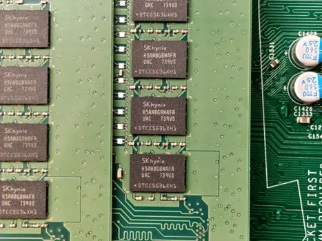
Each 1b/1c wafer reallocated to HBM or high-density server RDIMM removes that wafer from PC and mobile channels, and that is precisely what is happening in 2026. TrendForce data shows DRAM industry revenue rose approximately 81% quarter-over-quarter in 1Q26 while bit shipment growth remained constrained, which is the textbook signature of an ASP-driven, mix-driven cycle rather than a volume-driven one [S5]. Conventional DRAM contract prices climbed 90–95% QoQ in 1Q26 and were projected to rise another 58–63% QoQ in 2Q26, with Gartner's April 2026 forecast placing full-year DRAM price growth at 125% [S4][S5].
The segment split inside that mix is stark. Server DRAM is the priority allocation target, with North American CSPs locking in supply via long-term agreements to support future capacity expansion [S4]. PC DRAM faces an unusual situation: overall system demand has been revised downward, yet suppliers have simultaneously cut shipments to PC OEMs and module makers, forcing lower-allocation OEMs to procure at spot premiums [S4]. Mobile DRAM is squeezed on both sides, with weak smartphone unit demand offset by rigid AI feature requirements in flagship devices [S4]. Chinese retaliation against US HBM export controls has further fragmented allocation, raising compliance costs for multinational procurement teams [S4].
Side-by-Side: 1b vs 1c Across Decision Criteria
Three criteria separate 1b and 1c as of 2026: cost-per-bit position, EUV layer count and tool exposure, and product-mix fit. 1c carries a lower cost-per-bit potential than 1b in steady state because of the additional shrink step, but in 2026 the practical advantage is concentrated at SK Hynix, where the 1c mix is being pushed past 50% of domestic general-purpose output [S2]. 1b has the advantage of proven EUV-enabled yield and is the volume workhorse at Samsung and at Micron's 1β equivalent, which is why suppliers are running 1b and 1c in parallel rather than flipping in a single cutover [S3][S5].
The product-mix criterion matters as much as the cost criterion. 1c is the leading node for HBM4 base dies and high-density DDR5 RDIMMs, while 1b covers the bulk of DDR5 UDIMMs, LPDDR5X for mobile, and entry-level HBM3E stacks. Both nodes are gated by the same EUV tool lead-time constraint of 12–18 months [S5], so any new fab capacity tied to 1b or 1c effectively cannot reach meaningful production volume before late 2027, which is why NAND Research's May 2026 update places the relief horizon at late 2027 or 2028 [S4]. The DDR4 chip-vs-module inversion seen in late 2025, with DDR5 chip prices rising from $6.84 in September 2025 to $27.20 in December 2025, is a direct downstream consequence of 1b/1c wafers being steered away from DDR4 lines [S4].
Why 1b/1c Migration Is the Bottleneck, Not the Cure

The 1b/1c node migration is both the source of the shortage and the only credible path out of it, which is the structural paradox of the 2026 cycle. Capital intensity per wafer has risen on the advanced nodes and on 200-plus-layer 3D NAND, slowing capacity additions and making every wafer more expensive to bring online [S4]. The cost of a new DRAM fab remains in the $15–20 billion range with a 2–3 year build cycle, which means the 1b/1c capacity additions announced today will not move the supply needle until late 2027 at the earliest [S2][S4].
There is also a yield penalty baked into the node curve. DRAM density has stagnated at roughly 2× per decade versus the 100× per decade peak, and capacitor aspect ratios approaching 100:1 plus tens-of-thousands-of-electron charge levels mean that bitline and sense-amp signal margin is now the dominant yield constraint at 1c [S1]. The DRAM cell, at 6F² per bit, scales with the square of the half-pitch, so the bit-density gain from going 1b to 1c is meaningful but is not a doubling in the way earlier generations delivered, and the capex required to capture that gain is non-trivial [S3].
Who This Cycle Is For, and Who Gets Squeezed
1b/1c migration rewards the three majors that already have EUV-enabled capacity and HBM product roadmaps, and squeezes Tier-2 suppliers without HBM and the PC, mobile, and consumer channels that lose wafer allocation to AI server demand. SK Hynix is the most explicit beneficiary on the mix metric with its 50%-on-1c target for domestic general-purpose DRAM by year-end 2026 [S2]. Samsung and Micron sit alongside SK Hynix as the three suppliers able to actually shift 1b/1c mix at scale [S3][S5].
Buyers without multi-quarter long-term agreements are the structural losers of 2026 because spot exposure now carries extreme premiums, and even Tier-2 suppliers like Nanya are sitting on the sidelines on capex, a signal that the pricing umbrella is not yet wide enough to pull new conventional-DRAM capacity online [S4][S5]. Customers evaluating process instrumentation for new fab builds, including pressure transmitter selections for EUV vacuum and gas-delivery skids, flow meter sizing for ultra-pure water and slurry loops, and checking and testing apparatus for 1b/1c wafer acceptance, should plan for late 2027 as the earliest realistic window for fresh DRAM capacity, and price that into multi-year procurement contracts.
Trackable Signals for the Rest of 2026 and into 2027
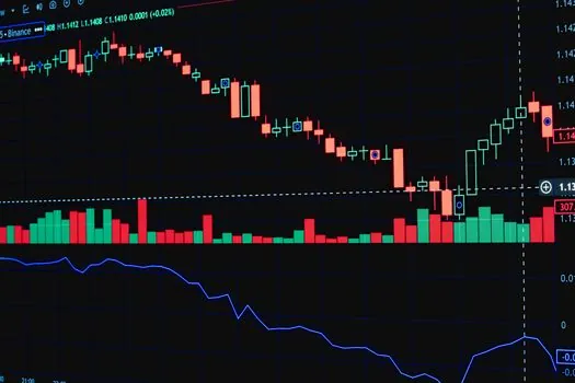
Three signals are worth watching through the end of 2026. First, SK Hynix's actual 1c share at year-end against the 50% target for domestic general-purpose DRAM [S2]. Second, Nanya's capex stance: a material acceleration would historically precede an oversupply cycle by 18–24 months, which would be the first credible signal that the oligopoly's pricing umbrella is breaking [S5]. Third, the timing of new fab capacity reaching meaningful production volume, which NAND Research places at late 2027 or 2028 [S4]. The DDR4 vs DDR5 contract-price inversion visible into 3Q26, including the Q3 50% jump and the chip-module inversion pattern, will be the cleanest read on whether advanced-node migration is easing legacy channel pressure or simply starving it further, a dynamic that mirrors how critical mineral stockpiling shifts buyer risk in 2026 for adjacent supply chains.