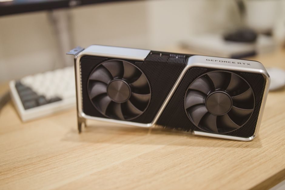
GPU bill-of-process cost decomposes into three primary buckets — wafer fabrication, advanced packaging, and final test — and the relative weight shifts dramatically with process node, HBM stack count, and package type (CoWoS-S vs CoWoS-L). At 4N/5nm class, foundry wafer cost alone typically accounts for the largest single line item, while 2.5D advanced packaging has become the second-largest cost driver for AI accelerators [S1][S4].
NVIDIA's AD102 GPU die is fabricated on TSMC's 4N process — a custom variant of N5 optimized for gaming and compute throughput — and ships in packages such as the L40 and L4 data-center SKUs that integrate GDDR6 memory subsystems on-substrate [S4]. The 4N node anchor is critical because it sets the per-die cost floor; every downstream packaging and test step is denominated against it.
Wafer Fabrication: Mask, Wafer, and Yield Cascade
At advanced nodes, mask set cost is the first non-recurring engineering (NRE) line item — full mask sets at 5nm and below run into the tens of millions USD per design, and they amortize across wafer volume [S1]. Wafer cost per unit scales with reticle count, EUV layer count, and wafer size (300mm standard for leading-edge GPU production).
Gross-die-per-wafer and functional-yield-per-die determine effective die cost. As a reference anchor, NVIDIA AD102 ships a 608.4 mm² monolithic die on 4N [S4] — a die size that inherently limits units-per-wafer versus smaller data-center dies, raising per-die fab cost before packaging markup. The 4N process is described in the Ada architecture whitepaper as delivering efficiency improvements over the prior N8 node powering Ampere, with the memory subsystem and power efficiency explicitly tied to the 4N manufacturing process [S4].
Pre-silicon IP licensing and analog/mixed-signal IP — high-speed SerDes, PLLs, ADCs/DACs — is a parallel cost line that fabless GPU vendors pay to third parties. Vendors such as VeriSilicon, InCirT, and Chain-IC provide licensable SerDes, PLL, and data-converter IP cores that get integrated into ASIC/SoC designs, with royalty structures layered on top of wafer cost [S1]. For a GPU SoC integrating PCIe Gen5, NVLink, and HBM PHYs, PHY IP licensing alone can reach seven figures USD per project.
Advanced Packaging: CoWoS, HBM Stacking, and Substrate Cost
CoWoS (Chip-on-Wafer-on-Substrate) is the dominant 2.5D packaging flow for AI GPUs, and its capacity-constrained supply has become a structural cost driver in 2024-2026 [S1]. The interposer area, HBM stack height (typically 8-Hi or 12-Hi for current-generation accelerators), and substrate layer count all scale package cost non-linearly.
Per-package cost for a CoWoS-S flow with 6-8 HBM stacks is widely reported in industry cost models as multiple times the cost of a conventional monolithic flip-chip BGA package at the same silicon area. CoWoS-L (with local silicon interconnects and RDL-based bridging) is the next-step escalation, used for the largest accelerator dies, where reticle-stitching and multi-chip disaggregation drive packaging cost toward half of total bill-of-material in some configurations [S1].
For NVIDIA's data-center SKUs like the L40, the package integrates GDDR6 memory rather than HBM, lowering the packaging cost versus HBM-equipped accelerators but also limiting memory bandwidth ceiling [S4]. The cost trade-off between HBM stacking (higher BOM, higher bandwidth) and GDDR6 (lower BOM, lower bandwidth) is a primary design decision that propagates into both performance tier and target market.
Test, Quality, and Yield-Driven Cost Multipliers
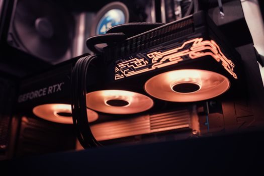
Final test (FT) and wafer-level burn-in (WLBI) costs scale with test time per die, the number of test insertions, and known-good-die (KGD) yield for HBM stacks and base logic die. GPU test engineering roles, such as the (COMPANY NAME) Arc Retail GPU Test Engineer position, focus on developing test plans, defining test equipment requirements, and driving root-cause analysis on failures — reflecting how test cost optimization is an ongoing engineering investment [S3].
Test cost is often expressed as a multiplier on raw die cost. HBM KGD yield is a specific pressure point: an 8-Hi or 12-Hi stack failing pre-bond test kills both the stack and the wasted interposer area.
System-level test (SLT) — running the GPU in a thermally realistic configuration under workload — adds another cost layer but is increasingly mandatory for data-center SKUs where field failure cost dwarfs the SLT line item. Quality assurance specifications at the fabless level also govern the QA stack, as detailed in GPU Manufacturing Quality: Fabless Fab, Brand-Level QA Stack, which covers brand-level test coverage and reliability protocols.
Comparison: Cost Driver Weights by GPU Class
Cost structure varies sharply by product class. A consumer gaming GPU on 4N with GDDR6 (e.g., AD102-based GeForce SKUs) allocates the largest share to wafer fab, with packaging in the conventional flip-chip BGA range and test as a moderate fraction. A data-center AI accelerator on CoWoS-S with 8-Hi HBM3 shifts the cost mix: packaging and HBM can approach or exceed wafer fab cost, with substrate/interposer becoming a first-class line item [S1][S4].
Three decision criteria frame the comparison: (1) process node cost per mm² — 4N is a custom TSMC variant optimized for Ada, so it does not map 1:1 to standard N5 wafer pricing [S4]; (2) memory type — HBM vs GDDR6 changes both BOM and bandwidth-per-dollar; (3) package complexity — monolithic BGA vs CoWoS-S vs CoWoS-L escalates packaging cost by an order of magnitude between tiers. For context on adjacent process industries, Industry 4.0 in 2026: What GPU Process Plants Spec for Smart Manufacturing details the smart-factory integration layer that influences yield management and cost control in modern fabs.
The NVIDIA Ada whitepaper explicitly lists "4N Manufacturing Process and Power Efficiency" as a dedicated section, indicating that process selection, power efficiency, and ultimately cost-per-performance are co-designed rather than treated as independent variables [S4]. This is the core engineering insight: GPU cost is not a single number, it is a stack of interdependent decisions, and node, memory, and package choice must be evaluated together.
Standards, Sourcing Constraints, and Cost-Driver Tracking Signals
There is no single industry standard governing GPU manufacturing cost reporting — cost data is fragmented across foundry pricing (TSMC, Samsung Foundry), OSAT packaging quotes, and HBM supplier (SK hynix, Samsung, Micron) negotiations. Public benchmarks come from teardown analyses and analyst models rather than audited disclosures. The IEEE and JEDEC standards that govern HBM (JEDEC HBM3, HBM2E) and package thermal/mechanical interfaces set performance and reliability baselines but not cost structures [S4].
Two trackable signals indicate cost-direction in 2026: CoWoS capacity expansion at TSMC and OSAT partners, and HBM3E/HBM4 qualification timing. CoWoS-S capacity remains the binding constraint for AI accelerator shipments through 2026, which means packaging cost will not deflate until supply normalizes — the GPU Manufacturing Quality: Fabless Fab, Brand-Level QA Stack analysis flags this as a sourcing risk. HBM3E ramp in 2025-2026 is a cost-down signal on a per-GB basis as 8-Hi and 12-Hi stacks move to higher density per stack.
Adjacent supply-chain pressure points also feed into GPU cost: rare-earth and substrate raw material costs, covered in Rare Earth Raw Material Sourcing Guide 2026: Spec Bands, Suppliers and Standards, apply to advanced packaging substrates and thermal interface materials, while ESD protection tooling and cleanroom consumables — covered in Anti-Static Equipment Price & Cost Guide 2026 — are a smaller but non-negligible line item in fabless back-end test operations.
Where the Cost Stack Breaks: Failure Modes and Limits
[S1]
Packaging failure modes include interposer defects (CoWoS-S), TSV misalignment in HBM stacks, and substrate warpage on large-area packages (CoWoS-L). Each of these drives scrap cost that gets amortized into the surviving-unit price. Test coverage gaps — missing a marginal tensor-core path or HBM PHY lane — translate to field RMA cost that exceeds the SLT savings, making test-coverage discipline a cost-control lever, not a quality afterthought [S3].
The realistic cost-reduction ceiling for advanced-node GPUs in 2026 is bounded by EUV throughput, HBM stack height (silicon-cap-limited at 12-16-Hi in current production), and CoWoS-L interconnector yield. Architectural moves toward chiplet disaggregation (e.g., NVIDIA's own GB/RGX-class partitioning in some SKUs) can reduce monolithic die cost but add packaging integration cost — net effect is GPU-class-dependent, not a universal win.
Final node: the cost stack is not "the wafer" or "the package" in isolation; it is the coupled function of node, memory, package, and test discipline. The next trackable signal is TSMC's N3-class ramp and how 4N volumes are re-priced as Ada's successor architectures move to N4P/N3 — a shift that will reflate the fab line item while potentially compressing packaging cost if CoWoS capacity normalizes. Monitor HBM4 qualification milestones through 2026-2027 as the second independent variable.
For component-level specifications, see additive manufacturing material, pressure transmitter, and flow meter.