Commercial photovoltaic (PV) cells are dominated by crystalline silicon, with monocrystalline Czochralski-pulled ingots feeding wafer sawing, while thin-film CIGS and emerging perovskite stacks add a parallel deposition route to the same module-assembly line [S1][S2].
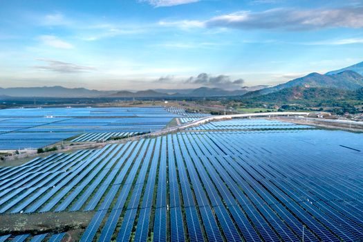
The defining economic metric in 2026 procurement is break-even system price per watt-peak ($/Wp): research for building-integrated PV places the average at roughly $3.2/Wp, climbing to about $4.5/Wp in lower-yield regions where capacity factors and irradiation drop [S2]. The same experience-curve analysis frames subsidies as the swing factor between commercial viability and stalled projects, and it is the most cited anchor for module-level cost engineering today.
Silicon Ingot and Wafer Production
Polysilicon feedstock (6N+ purity) feeds monocrystalline ingot growth in Czochralski pullers, where seed crystals draw boules typically 6-8 inches in diameter under argon at controlled thermal gradients; the alternative multicrystalline route uses directional solidification in quartz crucibles for higher throughput but lower carrier lifetime [S1].
Boules are squared, then wire-sawn with stainless-steel wire and slurry (or diamond-wire in newer lines) into wafers around 180 µm thick, with kerf loss historically consuming ~50% of the ingot mass. Wafer thickness has trended down toward 150 µm to stretch the same kg of silicon into more cells, which in turn raises mechanical-handling yield pressure downstream [S1]. For a process engineer, the bottleneck is no longer the grower but the wire-saw plus the post-saw wet etch that removes saw damage before texturing.
Cell Processing: From Wafer to Finished Junction
The standard crystalline-silicon cell is built around a p-type Cz wafer, with alkali texturing forming random pyramids, an n-type emitter diffused from a POCl3 source, a SiNx anti-reflection coating deposited by PECVD, and screen-printed silver front and aluminum rear metallization fired through the dielectric in a co-firing furnace [S1].
PERC (Passivated Emitter and Rear Cell) adds a rear-side Al2O3/SiNx passivation stack and a laser-opened local back-surface field, pushing production cell efficiencies into the 22-23% range for premium lines. For a procurement comparison on cell architecture: standard BSF (back-surface field) cells sit at ~19-20% mass-production efficiency, PERC at ~22-23%, n-type TOPCon/HJT at ~24-25% in pilot production [S1]. The trade-off is clean: every efficiency step costs capex in diffusion, PECVD, and laser tools, and that delta is exactly what shows up in the $/Wp figure.
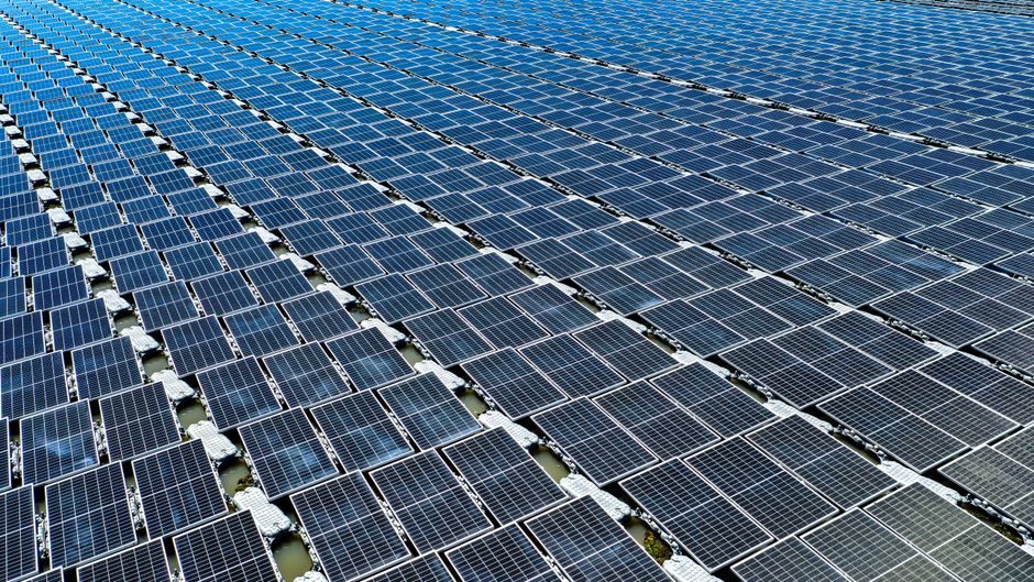
Module finishing is dominated by tab-and-string soldering of cells into 6x10 or 6x12 matrices, EVA/POE encapsulant encapsulation, a tempered low-iron glass cover, a back-sheet (or glass-glass in bifacial modules), and an aluminum frame with junction box. Flash-test sorting at STC (1000 W/m², AM1.5G, 25 °C) is the gate that defines nameplate watt-peak; mismatch losses between sorted bins typically add 1-2% to the string-level output if bins are mixed carelessly [S1].
Thin-Film Routes: CIGS, CdTe and the Perovskite Question
Copper indium gallium diselenide (CIGS) cells are deposited by co-evaporation or sputtering/selenization onto large-area glass or flexible foil substrates, reaching module efficiencies in the mid-to-high teens at production scale, with MiaSolé among the firms commercializing flexible CIGS at Solar Power International events for building-integrated applications [S3].
CIGS vs CdTe vs c-Si for utility-scale procurement lines up as: c-Si on cost and supply chain depth, CdTe on hot-climate energy yield, CIGS on flexibility and BIPV form factors [S3].
The 2025 analyst view cited on industry roundups is that solar-generated electricity reaches parity with natural-gas generation in most regions by 2025, with the implied module ASP trajectory as the supporting trend [S3].
Standards, Testing and Bankability Anchors
Module qualification and type approval are gated by IEC 61215 (performance), IEC 61730 (safety), and UL 61730 for the North American market, with IEC 61853-1/-2 covering energy-rating and measurement procedures; PID (potential-induced degradation) recovery is typically tested under IEC 62804, and salt-mist / ammonia resistance under IEC 61701 and IEC 62716 respectively. [S1]
For utility-scale procurement, the bankability package also includes a 25-year linear power-output warranty (commonly 97% year-1 and -0.7%/yr to year 25 for c-Si PERC), a Pmax tolerance of 0~+3% or 0~+5% depending on tier, and a bifaciality factor when bifacial glass-glass modules are quoted. A useful short verbatim claim from the underlying research: "the calculated average break-even price of PV systems for building-integrated applications is about $3.2/Wp, but can go up to about $4.5/Wp in areas with lower solar yield" [S2].
Process Control and Yield Levers in the Fab
The cell-fab bottleneck for a new PERC line is the PECVD passivation stack and the laser contact-opening tool: both are throughput-limited and both are yield-limited if the rear-side Al2O3 thickness drifts or the laser ablation leaves residue. Inline measurement of minority-carrier lifetime (µPCD or QSSPC), sheet resistance (four-point probe), and EL imaging under bias are the three tools a process engineer will not skip; an EL defect rate above ~2% usually maps to a co-firing or finger-printing problem, not a wafer problem. [S2]
Module-lamination yield is dominated by encapsulant cure cycle, vacuum integrity, and edge-seal quality; a typical EVA cure is 145-150 °C for 12-18 minutes, with cross-link degree above 80% required for weatherability.
Related Process Stacks in the Industrial Mix
PV fabs sit inside the same wider industrial process ecosystem as LED wafer-and-chip lines, where PECVD, sputtering, and cleanroom lithography are shared capital equipment categories. A side-by-side read of LED production workflows shows the same throughput-and-yield math, just with GaN instead of silicon and photon extraction efficiency instead of cell efficiency as the headline KPI. [S3]
On the project-finance side, utility-scale PV shares suppliers and contracting patterns with the offshore wind production stack — both depend on long-lead mechanical and electrical balance-of-plant, and both are now run on the same SCADA / industrial-control commodity hardware catalog that includes pressure transmitters for hydraulic pitch and cooling loops, flow meters for glycol and deionized-water balance, and PLCs as the cell-level controllers in the inverter-station auxiliary cabinets.
Trackable signals into the second half of 2026: n-type TOPCon/HJT capex announcements from the Tier-1 cell makers, the first bankable perovskite-silicon tandem field-data sets above 1 GW deployed, and a revised $/Wp break-even number from experience-curve updates as the polysilicon price floor stabilizes [S2][S3].