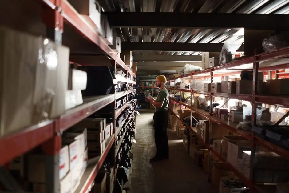
A MEMS sensor is not one chip but a four-stage chain: MEMS wafer fab, CMOS ASIC line, package/assembly, and test plus calibration, with each stage on a different node, different factory, and often different continent [S2][S4].
That four-stage split is the single biggest reason lead times and prices have stayed volatile: the 2021 MEMS and CMOS capacity squeeze pushed new product development cycles from roughly 12 months to up to 36 months by 2022, and pushed foundries that once accepted 300–1,000 wafer lots to either reject them or reprice them sharply [S4].
Stage 1, MEMS wafer fab: substrate choice sets the whole chain
The first decision is the wafer substrate, and it is the one that locks the rest of the supply chain: silicon dominates consumer and automotive inertial parts, while industrial pressure, high-temperature, and corrosive-service MEMS pull the chain toward silicon carbide, stainless steel, titanium, quartz, or specialized borosilicate glass [S4].
Mechanical feature size sits between 1 and 100 µm (with full device footprints typically 20 µm to 1 mm), and the suspended-mass plus capacitive-plate architecture is what makes a MEMS die a sensor rather than just an IC [S3]. Contamination rules are strict: traditional CMOS lines will not accept alternate substrates because sodium, transition metals, and dopants can diffuse into silicon, degrade gate oxide, lower minority carrier lifetime, and create PN junction leakage, so dedicated fabs for SiC, III-V, titanium, and stainless-steel diaphragms are built as standalone assets [S4].
A concrete industrial example: Japan-based Nagano Keiki runs an in-house sensor fab that machines each stainless-steel high-pressure diaphragm from rod stock, polishes the top, then runs the thimbles through trays on PVD and PECVD tools to deposit a doped polysilicon piezoresistive Wheatstone bridge, merging semiconductor thin-film processes with corrosion-resistant metal substrates for industrial and automotive pressure sensors [S4].
Stage 2, CMOS ASIC line: the partner fab that often gates shipments
Every MEMS die has to be paired with an application-specific CMOS ASIC for signal conditioning, analog front-end, and often the I2C, SPI, or interrupt-line interface, and that ASIC lives on a different fab process node, typically 0.18 µm to 40 nm CMOS, run by an entirely different foundry [S2][S4].
Capacity tightness in CMOS has historically been even worse than in MEMS, which is why a fabless MEMS startup with a working transducer can still be stuck: if the CMOS partner fab has no open slot, the BOM is half-built, and price is set by whoever owns the scarce tool [S4]. Customers that historically placed 300–1,000 wafer orders have been turned away or repriced, and small-volume fabless startups are the most exposed to that pinch [S4].
Selection tip for buyers: when qualifying a MEMS sensor for industrial UPS or switching power supply telemetry, ask the vendor which fab makes the ASIC and what node it sits on, because ASIC allocation is usually the binding constraint, not the MEMS die itself.
Stage 3, packaging and assembly: where MEMS parts die in the field
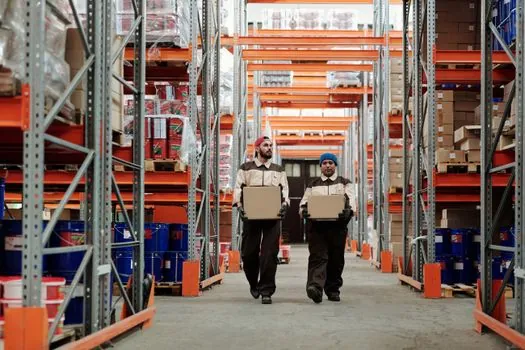
Packaging is the step that turns a fragile 1–100 µm mechanical structure into a module that survives -40 °C to +85 °C, IP65 or IP67 sealing, reflow, and years of vibration [S3].
A bare MEMS die cannot be dropped onto a board like a standard IC: the cavity, the gel fill, the getter, and the stress relief of the lead frame all determine whether the suspended mass drifts, the seal leaks, or the bias shifts across temperature. Sensor module makers therefore select a low-cost MEMS chip and add value through housing, connector, and calibration, and the more robust industrial module can carry 0.0001° digital resolution on a dual-axis inclinometer such as Jewell's JDI-100/200, with ±1° to ±60° measuring ranges, full temperature compensation from -30 °C to +60 °C, and 0.004° relative accuracy [S3].
Stage 4, test, calibration, and the More than Moore twist
Test and calibration is the fourth gate, and it is where MEMS differs most from a pure CMOS IC: every part has a mechanical offset that has to be zeroed, a temperature coefficient that has to be compensated, and a sensitivity that has to be trimmed against a reference stimulus [S3].
MEMS has also been pulled into the More than Moore (MtM) growth path, which adds wafer stacking, 3D structures, moving parts on a chip, and new wafer materials, the same recipe that gives wafer-level chip-scale packaging, optical micro-mirrors, and lab-on-chip fluidic structures, but it also means test tooling must handle stimuli the standard ATE cannot (pressure, acceleration, magnetic field, gas concentration, optical input) [S4].
A MEMS chip that is cheap on paper can triple in cost once the industrial-grade housing, connector, and three-axis test step are added [S3][S4].
Supply-chain risks and the materials that are hard to substitute

Three risks are structural rather than cyclical: alternate-substrate contamination rules that force dedicated fabs, university-to-fab transfer gaps for new materials, and ASIC allocation that gates MEMS shipments even when MEMS capacity is fine [S4].
If a new MEMS product needs a material set outside traditional silicon, moving a process out of a university fab and into industrial manufacturing is described as "almost impossible," because the equipment, contamination control, and process know-how do not exist on commercial CMOS lines [S4]. Borosilicate (BOROFLOAT), quartz, titanium, SiC, and stainless-steel diaphragm lines all live in dedicated fabs that are single-source by design, so a single fire, flood, or tool breakdown at one of those fabs can idle an entire sensor category for quarters, a dynamic that also shows up in non-electronic materials chains such as the synthetic resin supplier map.
For an engineer sourcing a sensor module today, the actionable signals to watch are: foundry disclosures on SiC and titanium capacity, ASIC partner fab node, and whether the sensor maker lists a university-process heritage, because each of those is a leading indicator of allocation, lead time, and the realistic second-source list.
For the relevant spec sheets and selection criteria, see power supply.