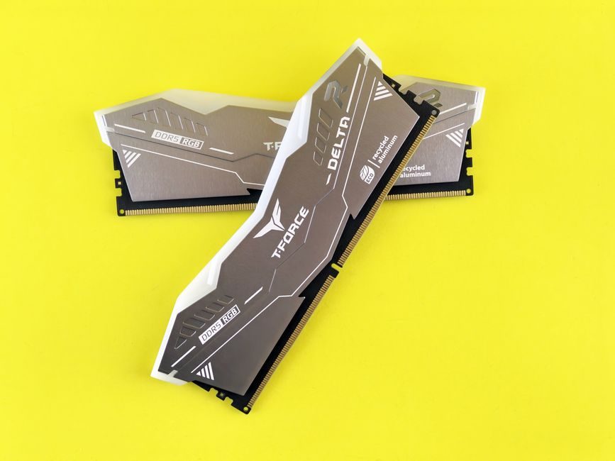
Q1 2026 global NAND flash market revenue reached $46 billion, nearly doubling sequentially and 3.5x the same quarter a year earlier, driven by sustained AI infrastructure demand according to Counterpoint Research tracking data [S2].
The trajectory mirrors the price surge DRAM experienced earlier in the cycle, with NAND ASPs now re-inflating after the 2024-2025 oversupply trough that pushed Samsung, SK hynix/Solidigm, Micron, and Kioxia/WD into coordinated wafer-start cuts [S2][S8]. China's YMTC entered volume sampling of its 128-layer 3D QLC/TLC parts to controller partners in 2020, putting domestic supply on the same node generation as Samsung, SK hynix, and Micron [S6].
Revenue and ASP Trajectory: From Oversupply to $46B
The Q1 2026 $46B revenue print is the highest quarterly figure on record for the NAND segment, a near-doubling quarter-on-quarter against Q4 2025 and 3.5x the Q1 2025 baseline according to Counterpoint Research's NAND market tracker [S2]. The prior downcycle that bottomed through 2024-2025 was severe enough that Micron, Kioxia/WD, Samsung, and SK hynix/Solidigm all announced capacity-utilization reductions and deferred node migrations to defend margins [S8].
The 2024-2025 inventory glut was driven by three factors: weak smartphone and notebook shipments, slower enterprise IT capex suppressing enterprise SSD demand, and channel inventory build that took multiple quarters to clear [S8]. The 2026 reversal is being attributed specifically to AI training and inference infrastructure, not consumer recovery, which structurally changes the demand mix toward high-density enterprise SSDs (read more on Top DRAM Memory Companies 2026: Samsung, SK hynix, Micron Capacity Map).
3D NAND Architecture and the Layer-Stacking Race
Modern NAND is a floating-gate non-volatile memory where each cell stores charge on an isolated gate and reads it back against a threshold voltage Vth; cell types range from SLC (1 bit/cell, 2 states) through MLC, TLC, to QLC (4 bits/cell, 16 states), with each step quadrupling-or-better density at the cost of endurance and signal margin [S5]. The industry has shifted from 2D planar to 3D vertical stacking, and the public roadmap from Samsung, SK hynix, and Micron targeted 128-layer TLC/QLC parts around 2020, with layer counts continuing to climb in subsequent generations [S6].
The economic logic of 3D NAND is straightforward: more layers per die means more bits per wafer without shrinking the cell pitch, which preserves endurance and reduces cost-per-bit. Samsung, SK hynix, WD, Micron, Kioxia, and Intel all benefited from 3D scaling, while YMTC (China) entered the generation with 128-layer 3D NAND samples shipped to controller vendors in 2020, putting it within one node of the established leaders [S6]. The ONFI standard and Toggle interface dominate the asynchronous/toggle command, address, and data protocols over the multiplexed 8-bit I/O bus that all NAND generations still rely on for bulk data transfer [S1][S4].
Cell-Type Trade-offs: SLC, MLC, TLC, QLC

The progression SLC -> MLC -> TLC -> QLC trades endurance and write speed for density and cost-per-bit. SLC's two states per cell give the widest Vth margin and the highest endurance, typically 100k P/E cycles, making it the choice for industrial, automotive, and boot-code applications where reliability dominates [S3][S5]. QLC's 16 states shrink the per-level Vth margin, cut endurance roughly 10x versus SLC, and demand more powerful ECC, but enable the lowest $/GB for cold storage and read-intensive AI datasets [S5][S6].
SPI NAND sits at the embedded low-density end of the market: industrial-grade SLC NAND packaged behind a serial peripheral interface that is pin-compatible with SPI NOR flash, giving embedded designers a higher-density, lower-cost-per-bit alternative when capacity requirements exceed what NOR can deliver [S3]. This is the segment where Chinese domestic suppliers have built a credible position, with SPI NAND listed alongside eMMC, eMCP, UFS, ePOP, and BGA SSD as a standard domestic storage product line [S3].
Vendor Landscape and Capacity Posture
The merchant NAND market is structurally an oligopoly: Samsung, SK hynix (which acquired Intel's NAND business as Solidigm), Micron, Kioxia, and Western Digital control the overwhelming majority of wafer output, with YMTC as the principal Chinese challenger [S6][S8]. The 2024-2025 cut actions were synchronized across this group, including utilization reductions and deferred node transitions, a coordinated discipline that the historical data file shows was the swing factor preventing ASP collapse to below-cash-cost levels [S8].
Capital intensity of 3D NAND (new fab modules, EUV-adjacent deposition and etch tools, hundreds of process steps per wafer) means that re-starting idled capacity takes 6-12 months, so even a sharp demand inflection like Q1 2026 cannot be met with immediate supply response. The result is the 3.5x YoY revenue jump driven entirely by ASP recovery on constrained wafer starts [S2]. For supply-chain engineers, this implies continued allocation pressure on high-density enterprise SSD part numbers through at least the next two quarters, a dynamic also visible across the DRAM side of the same memory cycle as tracked in the Top HBM Memory Companies in 2026: SK hynix, Samsung, Micron supplier map.
Industrial and Embedded Sourcing: SPI NAND and SPI NOR

For embedded and industrial buyers, the practical decision tree starts at interface and density. SPI NOR remains the default for low-density boot/parameter storage with byte-level random read and execute-in-place capability, but density above ~256 Mb and unit cost below SPI NOR's per-bit price push the design toward SPI NAND [S3]. SPI NAND's parallel to the SPI NOR command set means existing firmware stacks migrate with minimal rework, and the underlying SLC NAND die gives industrial temperature-grade reliability suitable for factory automation, railway, and energy applications [S3].
Domestic Chinese suppliers now publish complete SPI NAND product lines alongside eMMC, eMCP, UFS, ePOP, and BGA SSD, with industrial-grade SLC variants explicitly targeted at embedded ARM/PowerPC and X86 platforms [S3]. For specs engineers cross-referencing the broader industrial-component sourcing picture, the cost and lead-time dynamics on adjacent components are tracked in the Industrial Modem / DTU 2026 Price & Cost Driver Map.
Standards, Interfaces, and Cross-Generational Compatibility
NAND devices expose a heavily multiplexed 8-bit bus (I/O[7:0]) that carries command, address, and data in successive cycles, and the asynchronous interface defined by the ONFI (Open NAND Flash Interface) standard plus the rival Toggle interface from Toshiba/Kioxia are the two protocol families every controller must support [S1][S4]. Features such as LBA (logical block addressing) and Unique_ID are standardized across the ONFI specification, enabling per-die serialization for traceability and security use cases [S4].
NOR and NAND are not interchangeable. NOR's byte-level random access makes it execute-in-place capable (XIP, run code directly from flash), while NAND's page/block architecture delivers much higher write throughput and lower cost-per-bit but requires a flash translation layer (FTL) in the controller and cannot execute in place [S7]. Engineers migrating from SPI NOR to SPI NAND should plan for FTL integration, ECC engine tuning (BCH or LDPC depending on cell type), and bad-block management at the driver layer [S7].
Limitations and Watch Items for the Next Two Quarters
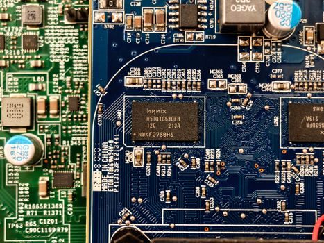
The Q1 2026 3.5x revenue print reflects ASP inflation on constrained wafer starts; the open question is whether AI infrastructure demand sustains or whether enterprise SSD orders normalize after hyperscaler capex digestion [S2]. On the supply side, the 2024-2025 utilization cuts create a 6-12 month lag before any capacity restarts can land incremental bits in the market, which structurally supports ASPs but also creates acute allocation risk for buyers on legacy part numbers [S8].
Trackable indicators for the next two quarters: (1) Counterpoint Research's quarterly NAND revenue print for Q2 2026 to confirm whether the $46B base extends or peaks; (2) the major vendors' (Samsung, SK hynix, Micron, Kioxia) wafer-start guidance and capex commentary in their Q2 earnings calls, which will signal whether the 2024-2025 cuts are being reversed; (3) the next 3D NAND node generation announcements, specifically any movement beyond the 128-layer baseline on the public roadmap, since layer-count step-ups historically reset the cost-per-bit curve and unlock new density tiers [S2][S6][S8].
Spec-level background on the components involved: pressure transmitter, flow meter, and industrial valve.