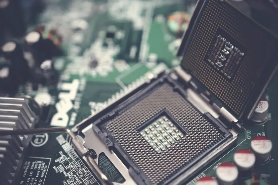
Power semiconductors (IGBTs, SiC MOSFETs, GaN HEMTs, and the gate drivers and isolated DC/DC converters around them) sit on a seven-stage global value chain that, in the words of CSIS, is as geopolitically consequential as oil and gas, with the Indo-Pacific region producing the largest share of leading-edge wafers [S1]. Annual semiconductor sales crossed half a trillion USD in 2022, and the U.S. Department of Commerce estimated the 2020-2021 chip shortage shaved about 240 billion USD off U.S. GDP, with U.S. auto output down 7.7 million vehicles that year [S1].
For process engineers specifying IGBT modules or SiC discretes, the supply chain is not an abstract flow chart: it dictates 12- to 26-week lead times, single-source exposure on photolithography, and a hard cap on how many 200 mm SiC wafers a fab can put out per month. The chain is also a long-cycle chain, where a wafer can spend up to six months in production before it reaches an ATP line [S3].
Seven stages from IC design to back-end test
CSET divides production into three core segments: design, manufacturing, and assembly/test/packaging (ATP), wrapped by an enabling ecosystem of materials, semiconductor manufacturing equipment (SME), electronic design automation (EDA), and core IP [S4]. Rabobank's mapping extends the timeline, noting that a single device can spend up to half a year moving through research, design, front-end wafer fab, and back-end assembly, packaging, and testing [S3]. TSMC's own value-chain diagram routes flow as System Companies, EMS, IC Design, IC Manufacturing, IC Assembly and Test, and End Consumers, in that order [S5].
For a power device specifically, "design" is split between fabless houses (often fabless GaN/SiC startups) and IDMs that own both fab and packaging. "Back-end manufacturing" covers dicing, die-attach, wire bonding or copper-clip bonding, molding, and final test, with discrete TO-247 packs, half-bridge modules, and full power-integrated modules each following different lines and tooling sets.
Geographic concentration and the chokepoints that actually bite
Rabobank's "Mapping Global Supply Chains, the Case of Semiconductors" finds that Taiwan and South Korea produce the bulk of leading-edge semiconductors, but their fabs depend on raw materials, specialty gases, photoresist, and lithography equipment that flow in from the U.S., Europe, and Japan [S3]. The Netherlands holds an outsized position because ASML is the sole producer of EUV lithography systems; a single EUV scanner costs more than 200 million USD and is required for sub-7 nm logic and many advanced power processes [S3]. Japan anchors silicon wafer production (Shin-Etsu, Sumco), photoresist (JSR, Tokyo Ohka), and high-purity chemicals, while the U.S. dominates EDA (Cadence, Synopsys, Siemens EDA), core IP (Arm, various RISC-V vendors), and much of the SME installed base outside lithography.
The single biggest chokepoint in the power device world is not EUV (most IGBT and SiC lines still run on 90-350 nm nodes) but rather 200 mm SiC substrate supply: only a handful of vendors can deliver production-volume 150 mm and 200 mm SiC wafers with low micropipe density, and substrate capacity is what gates SiC MOSFET output. Photoresist, advanced packaging substrates (ABF), and high-purity hydrogen, helium, and neon gases are routinely cited as the next layer of chokepoints [S3][S7].
Why power devices follow a different logistics rhythm than logic
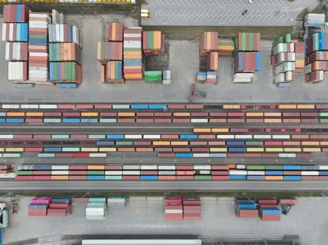
Power semiconductors are mostly mature-node (90-500 nm) and run on 200 mm or even 150 mm wafers, but they still inherit the same upstream bottlenecks as leading-edge logic: the same EUV-adjacent EUV-free ASML DUV scanners, the same photoresist supply, and the same gas and chemical vendors [S3]. A power module fab (IGBT, SiC) typically runs a 12- to 26-week wafer cycle, followed by 4-8 weeks of back-end assembly and burn-in. Long-cycle plus single-region exposure means a typhoon in Hsinchu, a gas contamination event in a Japanese specialty chemical plant, or a labor action at a Dutch SME vendor can move SiC MOSFET and IGBT lead times by two quarters in either direction [S3].
Compare that to advanced logic fabs, which run 300 mm wafers on sub-7 nm nodes with EUV: capital intensity is several times higher, but cycle time per wafer is not dramatically shorter, and a much larger fraction of unit cost sits in lithography and metrology. From a sourcing perspective, power electronics buyers face longer absolute lead times and fewer second-source options than the headline logic shortages would suggest.
Where power module and converter buyers actually plug in
End integration concentrates in China, where the largest share of finished devices is consumed in inverters, EV drivetrains, white goods, and industrial power conversion gear [S3]. A power-electronics OEM sourcing IGBT modules, SiC discretes, or switching power supply units therefore depends on at least three or four cross-border hops: SiC substrate (U.S./Japan/China) to epitaxy (U.S./Europe/Japan) to fab (Taiwan/Germany/U.S./China) to ATP (China/Southeast Asia) to inverter or industrial UPS integration (China, EU, U.S.).
For reference, the MEMS sensor supply chain runs through similar nodes but adds a CMOS-compatible fab step and a wafer-level packaging stage, which is why MEMS and power devices frequently share the same back-end ATP vendors in Taiwan and Malaysia. The specialty chemicals market map covers the photoresist, hydrogen, neon, and CMP slurry layer that sits just upstream of every fab, while a multifunction power meter sourcing map describes how the finished goods (the meters, drives, and UPS units that use these semiconductors) are distributed downstream.
Selection implications for power-electronics design
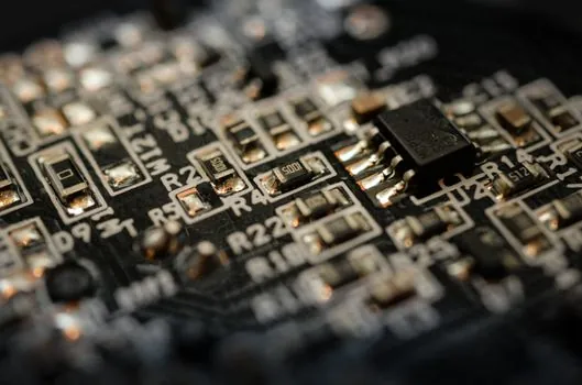
Three engineering decisions directly inherit supply-chain risk: topology, device family, and packaging. SiC MOSFETs offer the best efficiency at 650-1700 V but carry the highest 2026 wafer-substrate lead-time exposure, while IGBTs at 600-1700 V are sourced from a more mature multi-vendor base (Infineon, Mitsubishi Electric, Fuji Electric, ON Semiconductor, Starpower, CR Micro) with shorter quoted lead times. GaN HEMTs at 100-650 V are largely IDM- or foundry-driven (TSMC GaN, Power Integrations, GaN Systems, Innoscience) and are tightest on epitaxy capacity, not on the device fab step itself. [S5]
For a 50 kW to 1 MW industrial UPS build, the practical difference shows up in BOM risk register: SiC-based stages can carry 30-52 week lead times on 200 mm SiC substrates in tight allocation, while silicon IGBT equivalents typically ship in 12-24 weeks. Designers who can accept 2-3 percentage points of additional conduction loss can dual-source through silicon IGBTs; those who cannot, usually have to commit to a single SiC vendor and a 12-month forecast.
Limitations, failure modes, and what to watch
The biggest limitation in the published supply-chain literature is resolution at the device-family level. The CSIS, Rabobank, CSET, and TSMC charts all aggregate at the integrated-circuit level, not the discrete power-device level, so SiC and GaN share a box with IGBTs even though their substrate, epitaxy, and ATP lines are nearly disjoint [S1][S3][S4][S5]. A second limitation is the staleness of installed-base data: most of the cited numbers reference 2021-2023 conditions, and the 2026 picture (new U.S. fabs, China mature-node expansion, SiC capacity additions) is only partially reflected.
Trackable signals for the next quarter: TSMC and GlobalFoundries 200 mm and 300 mm SiC pilot-line output, Wolfspeed and Resonac 200 mm substrate yield disclosures, and any further ASML export-license decisions on DUV and EUV systems to Chinese fabs. Inventory normalization at distributors (Digi-Key, Mouser, Avnet) is the cleanest short-cycle indicator: IGBT and SiC MOSFET lead times dropping below 16 weeks would suggest the 2022-2024 allocation cycle has finally broken [S3].
For the relevant spec sheets and selection criteria, see power supply.