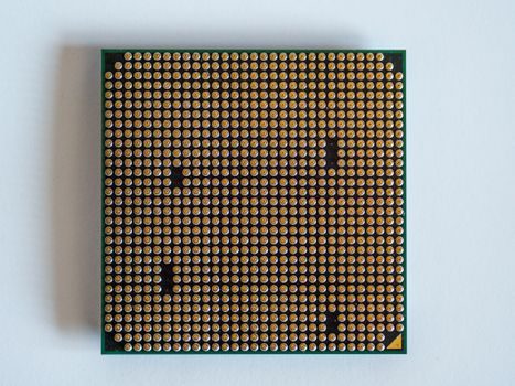
Modern semiconductor production is a two-stage industrial flow — front-end wafer fabrication (FEOL) and back-end packaging/test (BEOL) — executed on equipment sets that range from ASML EUV scanners to wire bonders, with process nodes now in volume at 3 nm and 2 nm logic and 200+ layer 3D NAND [S2].
The scope covered here is the manufacturing technology itself: lithography, etch, deposition, doping, CMP, metrology, dicing, packaging, and the power-device variants (SiC, IGBT, GaN) that branch off the same fab infrastructure. Selection criteria, equipment classes, and node-scale cost trade-offs are mapped against the 2026 capex cycle [S1].
Front-end process stack: lithography, etch, deposition
Front-end processing of a logic die takes 400–800 individual steps through photolithography, plasma etch, CVD/PVD/ALD deposition, ion implant, oxidation, diffusion, and chemical-mechanical polishing before the wafer reaches a probe test station [S2]. The lithography step defines the minimum half-pitch and is the rate-limiting capital line: ASML's EUV systems handle the critical layers at 7 nm and below, while ArF immersion handles the non-critical layers and trailing-edge nodes from 28 nm up to 14 nm.
Etch and deposition have scaled alongside lithography — atomic-layer etch (ALE) and high-aspect-ratio plasma etch are now standard for FinFET and GAA gate-all-around structures, and ALD delivers sub-nanometre film thickness control for the high-k metal gate stack and the multi-layer interconnect barrier/liner [S2]. The number of mask layers per die rose from ~30 at the 90 nm node to 80+ at 5 nm, which is the structural reason EUV layer count and EUV dose per wafer dominate the cost-per-die curve.
Node-scale comparison: 28 nm, 7/5 nm, 3 nm, 2 nm
The right node is dictated by performance-per-watt, die area, and wafer cost — not by the marketing number on a datasheet. A 28 nm planar CMOS wafer costs roughly a third of a 7 nm wafer per die area but delivers a fraction of the logic density, so high-volume consumer SoCs cluster at 7/5 nm while automotive MCUs, PMICs, and analog IP stay at 28/22/16 nm [S2]. At 3 nm, foundries reported a transistor density of around 200–250 MTr/mm², doubling roughly every two nodes; the 2 nm GAA nanosheet node moved from risk production into early volume over 2024–2025 and is the volume driver for the 2026 capex cycle [S1].
The trade-off stack: 28 nm offers the lowest defect density and best analog/RF performance per dollar; 7/5 nm gives the best logic density at a mature EUV layer count; 3 nm increases density but raises wafer cost; 2 nm GAA maximizes density but consumes the highest EUV dose per wafer and is the most sensitive to EUV pellicle and mask-blank yield. Power devices (SiC MOSFETs, IGBTs) do NOT follow the logic-node shrink curve — they are tied to 150/200 mm wafer fabs on older nodes, with a separate capex cycle, as covered in the 2026 SiC pricing and IGBT allocation analysis power semiconductor supply 2026: SiC pricing, IGBT allocation, and sourcing risk.
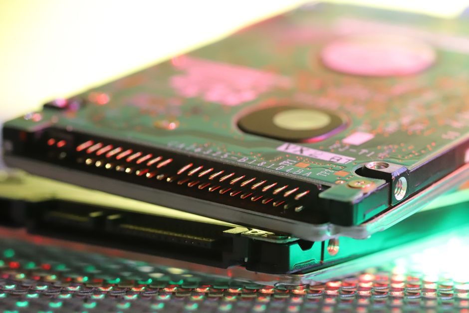
Back-end: dicing, packaging, test
After wafer-level test, the wafer is thinned (typically 50–100 µm for advanced packages), diced by diamond-blade or stealth-laser dicing, and the known-good die is mounted on a substrate or interposer. Wire bonding still handles the bulk of QFP/QFN automotive and industrial packages, while flip-chip BGA, fan-out wafer-level packaging (FOWLP), and 2.5D/3D die-stacking using TSV (through-silicon via) handle high-I/O logic and HBM-stacked memory [S2].
The advanced-packaging capex line is now comparable to the FEOL line for AI accelerators: TSMC's CoWoS-S/CoWoS-L lines, Intel's EMIB/Foveros, and Samsung's I-Cube are the production 2.5D/3D stacks in volume at 2026, and each interposer or bridge-die adds a separate metrology and bump-yield gate. For most industrial and automotive buyers, the practical selection is between standard wire-bond QFN (cheapest, lowest I/O), flip-chip BGA (mid-cost, high-I/O), and FOWLP (smallest footprint, thermal-sensitive), as detailed in the 2026 semiconductor smart manufacturing coverage on GEM300 and brownfield automation semiconductor smart manufacturing 2026: AI, GEM300, and brownfield automation stack.
Power devices branch: SiC, IGBT, GaN
Power semiconductors are NOT a sub-category of logic — they are a separate manufacturing technology track on 150/200 mm wafers, with thicker epitaxy (typically 5–15 µm SiC epilayer), higher thermal-budget steps, and packaging rated for 175–200 °C junction [S2]. SiC MOSFETs now dominate 800 V EV traction inverters and 1500 V PV string inverters because of the 10× lower switching loss versus silicon IGBT at the same voltage class.
The 2026 production reality: SiC wafer supply is the constraint, not the fab capacity — 150 mm SiC wafers remain the volume baseline and 200 mm SiC line capacity is still ramping, which is the upstream driver for the SiC price premium and the reason IGBTs are being specified longer than originally forecast for sub-200 kW industrial drives. GaN-on-Si is the third branch, used in 100–650 V high-frequency power conversion where the smaller die and faster switching justify the higher $/mm² cost. A wafer-fab smart-manufacturing stack that covers AI vision, GEM300, and advanced process control for both logic and power lines is profiled in the semiconductor smart manufacturing 2026: AI, GEM300, and brownfield automation stack piece.
Materials and supply chain: silicon, SiC, photoresist, EUV pellicles

The raw-material stack is dominated by single-crystal silicon (12-inch / 300 mm for logic, 8-inch / 200 mm for mature and power), single-crystal SiC (150/200 mm), photoresists (KrF, ArF, ArF-immersion, EUV chemistries), ultra-high-purity gases (NF₃, SiH₄, NH₃, HBr), CMP slurries, and sputtering targets. Each is a separate supply line, and the EUV pellicle is a single-source critical consumable — a yield-impacting failure mode that propagates across every 3 nm and 2 nm wafer [S1].
Selection of a fab process for an OEM product in 2026 maps to: (a) target node and wafer size, (b) logic vs memory vs power, (c) packaging style and pin/IO count, (d) AEC-Q100/Q101/Q104 automotive grade if required, and (e) minimum order quantity and second-source roadmap. Buyers who specify a node that does not match a foundry's high-volume ramp will pay a 2–4× wafer-cost premium — a non-trivial variable in the AI-chip smart manufacturing stack: edge compute, agentic AI, and GEM300 in 2026 capex context.
Limitations and failure modes in 2026 production
The dominant yield-killer in 2026 is multi-patterning stitching error and EUV stochastic defectivity at the 2 nm GAA node, followed by advanced-packaging bump-bridge yield at 2.5D interposers and by HBM stack warpage during thermo-compression bonding [S1]. For power devices, the dominant failure modes are SiC basal-plane dislocation propagation and gate-oxide TDDB at high dV/dt — both are lifetime limiters for traction inverters and are not fully captured by standard AEC-Q101.
Equipment throughput is the second constraint: a single EUV scanner at the 2 nm dose delivers ~150–180 wafers per hour, and the EUV source power, pellicle replacement, and qualification outages are the largest contributors to wafer-cost variance. Buyers who need second-source 2 nm capacity in 2026 should verify that the foundry has a non-EUV fallback layer set, since the 2 nm GAA tape-out assumes EUV at every critical layer — there is no dry ArFi escape route on this node [S2]. The full semiconductor manufacturing process: front-end, back-end, and node-scale flow for 2026 article maps these failure modes to the equipment and process steps that generate them.
Sourcing signals to track in 2026
Trackable signals for the back half of 2026: foundry monthly wafer-out by node, 200 mm SiC wafer merchant supply, EUV pellicle second-source qualification, and CoWoS/SoIC packaging line ramp at the major foundries — each is a leading indicator of wafer-cost movement and lead-time at the buyer level. [S1]
For component-level specifications, see pressure transmitter, flow meter, and industrial valve.