The solar and semiconductor value chain begins with raw silicon ore, escalates through a purification stage (such as the Fluidized Bed Reactor process) to produce super-pure silicon, and exits the wafer fab as polished wafers that downstream fabs convert into solar cells and diffused-wafer transistors/diodes used in electric power control devices [S1][S2].
Cost and spec pressure travel downstream in one direction: upstream purity and diameter decisions lock in wafer flatness, bow, total thickness variation (TTV) and minority-carrier lifetime, which in turn set the upper ceiling for solar cell conversion efficiency and the leakage current budget for 12-inch logic wafers [S1][S2].
Upstream Tier: Metallurgical Silicon, Polysilicon, Crucibles and Field Instruments
Quartzite mining and Siemens-process polysilicon plants sit at the head of the chain, with trichlorosilane (SiHCl3) fluid beds and bell-jar reactor gas flows measured by rotameters, Coriolis and electromagnetic flow meters at the reactor inlet and recycle loop [S1]. In solar-grade wafer lines, NaOH/KOH etching baths and HCl/HF acid mixture ratios are the most heavily metered wet-chemistry streams, and Yokogawa application notes cite rotameter use on the wet bench as a calibrated, repeatable choice where line size, viscosity and clean-room footprint justify a mechanical variable-area meter over a more complex Coriolis [S1].
Polysilicon rod diameter (typically 150-200 mm), chunk morphology and surface metal contamination (Fe, Cu, Na, K each typically targeted below the ppb level for solar-grade feedstock) define the maximum carrier lifetime downstream — a polysilicon lot with high bulk metal cannot be rescued by better wire saw tuning. For the cylindrical Czochralski pullers and directional solidification (DS) blocks downstream, the dominant field-instrument topics are loop pressure stability on the argon inert shroud, heater-zone thermal profiling, and hot-zone vacuum integrity [S1][S2].
Mid-Stream Tier: Crystal Growth, Slicing, Lapping and Polishing
Czochralski (CZ) pulling for IC wafers targets 300 mm diameter ingots weighing roughly 300-400 kg; the DS blocks used for p-type mono solar wafers now exceed the G12 format (182 mm × 182 mm pseudo-square cells), and the wafer thickness moved from 180 µm down to 150 µm and 130 µm in 2024-2025, with N-type TOPCon and HJT lines running 120-130 µm [S1]. Diamond wire saws use 50-80 µm brass-coated wire at 1,500-1,800 m/min web speed, and kerf loss is the single largest silicon-yield lever — narrower wire and lower TTV both depend on the upstream flow and temperature uniformity of the slurry [S1][S2].
After slicing, the wafer must hit a TTV below 5 µm for solar and below 3 µm for IC, with surface roughness Ra typically below 0.5 nm post-CMP. For mono wafer ID and downstream traceability, the wafer-handling robotics, FOUP/FOSB stockers and the linear modules in those cassette elevators run on stroke-length and payload benchmarks identical to the ones we tracked in 2026.
Downstream Tier: Solar Cells, Power Devices and Integrated Circuits

Solar-cell lines consume the bulk of p-type mono wafers and convert them into PERC, TOPCon and HJT modules; commercial TOPCon module efficiencies sit in the 23.5-25.0% band, and the metal-ink screen-printer alignment tolerance is on the order of ±10 µm, which is why wafer TTV and bow must be held so tightly upstream [S1]. For IC and power electronics, the same 200/300 mm polished wafer is split into logic, memory, and discrete-device lines; silicon nitride, silicon carbide and silicon steel (electrical steel) are the three adjacent engineered substrates that compete in EV inverters, traction motors and high-frequency magnetics — readers building a motor-drive bill of materials will see overlapping sourcing logic across these substrates, as covered in our electrical steel and electrical-grade silicon overview and the silicon carbide wafer and epitaxy primer.
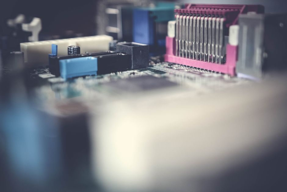
The fab-level gas panel and slurry distribution subsystem is another place where downstream capacity ties back to mid-stream wafers: mass-flow controllers (MFC) on SiH4, N2O and NF3 lines, pressure transmitters on the slurry day-tank headspace, and a flow meter on the CMP slurry return line all sit inside the same tool as the wafer-handling robot.
Selection Criteria by Application Path
For solar-grade mono wafers, the four binding spec gates are: minority-carrier lifetime (typically above 1,000 µs for n-type HJT substrates), thickness (120-150 µm), TTV (≤5 µm), and bow (≤40 µm). For 200 mm/300 mm IC wafers, the gates shift to: resistivity grade (p-type 1-100 Ω·cm for logic, 0.001-0.1 Ω·cm for power discretes), surface metal contamination (each species below 1×10⁹ atoms/cm²), and bulk oxygen/carbon concentration (oxygen typically 10-18 ppma for internal-gettering wafers, below 8 ppma for low-oxygen epitaxial substrates) [S1][S2].
A 150 mm SiC wafer still costs multiples of a 200 mm silicon wafer in 2026, but its 1,200-1,700 V/µm breakdown field versus silicon's ~300 V/µm is what lets an EV inverter shrink the bus capacitance and the cooling plate at the same time.
Limitations, Failure Modes and Sourcing Constraints

The three recurring failure modes along the chain are: (1) wire-saw marks propagating into cell efficiency at 0.5-1.0% absolute conversion loss if the slurry chemistry drifts; (2) metal contamination from the quartz crucible lifetime, where a worn crucible can spike Fe/Cu/Na to the ppb range in a single batch; (3) downstream slurry pressure pulsation driving wafer-chuck slip, which is a pressure transmitter damping and MFC bandwidth problem, not a wafer problem. Sourcing-wise, the constraints in 2026 are dominated by polysilicon capacity, quartz crucible supply (key nodes in GE Quartz / Momentive-style fused-silica lines), and 12-inch wafer epi-reactor lead time, with diamond wire and slurry abrasives tracked through the industrial valve and chemical-dosing stack on the wet bench. [S1]
For supply-chain research at the chain level, the Wind Product Database documents 5,154 industry nodes and 160,000+ upstream-downstream relationships across A-share, H-share and major US-listed names [S3]; in practice, a wafer-fab buyer maps their bill of materials into that chain to find which single-source nodes (high-purity polysilicon, fused quartz, 12-inch epi reactors, MFCs) carry the highest lead-time risk.
Instrumentation Touch-Points Across the Chain
Rotameters on wet-bench acid lines, Coriolis meters on polysilicon reactor recycle, and flow meter skids on the slurry return line are the three instrument signatures that show up at every tier [S1]. The wet-bench rotameter choice is a useful proxy: Yokogawa's application note positions the variable-area meter as a calibrated, low-maintenance pick for HF/HCl mixing where a magnetic or vortex meter would suffer from chemical compatibility or low-flow resolution issues, and the same reasoning recurs at the gas-panel boundary where thermal MFC and Coriolis each take a different segment of the flow range [S1].
On the gas panel, hydrogen, silane and ammonia lines typically run at low single-digit sccm to a few slpm, and on-site auditing repeatedly shows that MFC zero-drift, not the pressure transmitter head, is the limiting factor on epitaxial layer thickness uniformity. Across the chain, the dominant procurement signals in 2026 are MFC lead time (multi-quarter for certain ranges), rotameter float material selection (PTFE, sapphire, Hastelloy), and ICP-MS contamination monitoring on the polysilicon feedstock — all of which sit upstream of the wafer spec itself.
Closing note: the next trackable signal for buyers is the 12-inch wafer epi-reactor lead time quoted in Q3 2026 versus the 150-200 mm line, because a 30-60-day shift there propagates directly into 200/300 mm wafer allocation for the 2026-H2 fab cycle; second, watch the slurry-day-tank headspace-pressure telemetry band, which is the easiest on-site indicator of CMP slurry outgassing and a leading signal for downstream wafer-handling slip.