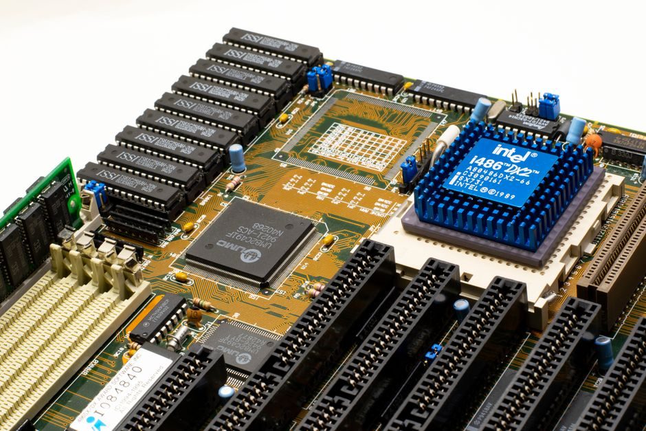
A modern processor is governed by three overlapping bills of materials that engineers must track separately: a silicon BoM (die, cores, cache, integrated memory controller, GPU/AI accelerators, PCIe/USB PHYs), a package BoM (substrate, solder bumps, integrated heat spreader, TIM, socket or BGA), and a software BoM — firmware, microcode, boot ROM, bootloader, drivers, BSP and the RTL/IP that produced the silicon [S1].
For an SoC or a server-class CPU, the software BoM is not an afterthought: it is a complex stack of firmware, bootloaders, microcode, drivers and Board Support Packages (BSPs) that Perforce explicitly identifies as part of the deliverable bill of materials under modern SBOM practice (SPDX / CycloneDX) [S1]. Procurement teams that ship a hardware-only BoM to compliance reviewers leave the largest attack surface — the signed microcode patch, the ME/PSP firmware blob, the secure-boot chain — undocumented.
Silicon die: cores, cache, uncore and the I/O ring
The die is the monolithic block of single-crystal silicon whose fixed logic structure carries the L1/L2/L3 cache, execution units, instruction decoders, register files, branch predictor and the bus interface to the outside package [S5]. Processors in the same family can share an architecture (instruction set, ISA extensions, cache hierarchy) but differ in core count, frequency, cache size and integrated graphics; an 8-core desktop part and a 6-core variant of the same silicon are the same die with two cores disabled and a different fuse map, not a different BoM.
Critical die-level BoM lines a sourcing engineer has to list line-by-line: process node (e.g. a 5 nm or 3 nm FinFET class), reticle count, number of CPU cores, unified L3 capacity, integrated memory controller generation and channel count, PCIe lane count and generation, integrated GPU execution units, NPU/AI accelerator TOPS, and the I/O die (IOD) in chiplet layouts [S3]. Front-end fabrication (silicon wafer → blank die) and back-end test (wafer sort, burn-in, bin by leakage/ frequency) both feed the same die BoM but are usually billed to different cost lines.
Package and interposer: the second BoM
The package is what turns a fragile bare die into a component a contract manufacturer can solder; for high-end CPUs it includes the organic substrate, C4 solder bumps or copper pillars, a heat-spreader lid, two layers of thermal interface material (TIM1 between die and lid, TIM2 between lid and cooler) and either a pin-grid-array socket or a BGA land pattern. Modern server and client CPUs ship in multi-chip packages where one or more compute dies sit next to an I/O die on a silicon interposer or on an embedded multi-die interconnect bridge (EMIB); the interposer itself is a sourced line item with its own wafer foundry. [S1]
Materials and tolerances to capture in the package BoM: substrate layer count (typically 4-12 for client, up to 20+ for server), bump pitch (130-150 µm in current client, 100 µm class on leading-edge server PHYs), IHS material (nickel-plated copper for most desktop/server, omitted on mobile for height), and socket land pattern / pin count (LGA 1700 class for client, LGA 4677/4189 class for server) [S3]. Reference coverage of how chiplet interposers and HBM stack side-by-side with CPU dies is consolidated in the AI chip BoM 2026 teardown at AI chip BoM 2026: HBM, CoWoS, EUV wafers and the dual hardware/software BoM.
Hardware BoM vs Software BoM: split ownership
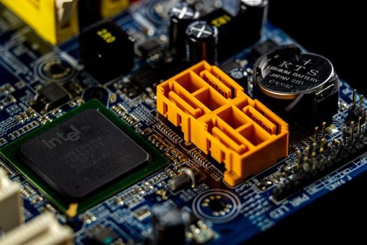
A compliant CPU bill of materials in 2026 must be split, not merged, because the two halves have different suppliers, different version cadences, and different vulnerability windows. The hardware side is owned by the fab, the OSAT and the substrate vendor; revisions move on a yearly cadence tied to process shrinks and packaging shrinks. The software side is owned by the silicon vendor's firmware team plus the BSP/mainline-Linux maintainers; microcode, AGESA/ME/PSP blobs and bootloader can be patched monthly [S1].
Concrete lines a procurement audit should demand on the software side: microcode revision (e.g. the signed patch level loaded at boot), ME/PSP firmware version, BIOS/UEFI image and capsule update channel, RCPL/safty microcode fuse map, and the list of third-party IP blocks delivered as RTL/encrypted netlists (PCIe controller, USB PHY, display pipeline) [S1]. Skipping any of these turns the "BoM" into a marketing datasheet; for an engineering reference, a missing line is a known-unknown risk that downstream CMMC and supply-chain reviews will flag.
Selection criteria and what the BoM tells you about price
Three parameters move the vast majority of CPU unit cost and they are all visible in the BoM: die size in mm² (which scales roughly with core count and cache), package tier (client vs server, BGA vs socketed, with or without integrated heat spreader), and the firmware/software support window the vendor commits to. A 10% larger die at the same process node typically costs 8-15% more once defect-density yield is factored in, which is why a 6-core and an 8-core SKU are usually cut from the same wafer and only the enabled fuses differ. [S2]
For content-creation and productivity workloads the BoM trade-off is shifting: a high-efficiency modern core on a recent node with a strong NPU often beats a peak-frequency older part on a mature node, because the NPU and media engine offload decode, upscale and noise reduction from the CPU cores — that is the explicit framing of the June 2026 channel-creator CPU guide [S7]. A BoM-driven sourcing decision has to weight TOPS-per-watt, supported memory speed (DDR5-5600 vs DDR5-8000 class) and the platform's PCIe 5.0 lane count, not only frequency and core count.
Comparison of the three BoM layers
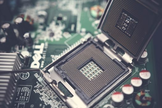
Lining the three BoM layers against the same four engineering criteria shows why they cannot be merged into one spreadsheet. (1) Lead time: silicon die 12-26 weeks from wafer start, package 4-8 weeks, software BoM (firmware/BIOS) hours to days from a vendor repo [S1]. (2) Cost driver: die area and process node for hardware, package tier for assembly, engineering labour for software. (3) Failure mode: silicon defect or timing-margin miss for die, solder-joint fatigue or substrate delamination for package, signed-microcode rollback or boot ROM CVE for software. (4) Compliance owner: foundry/OSAT, OSAT/CM, silicon vendor security team.
This separation maps directly to the supply-chain roles an OEM must assign; it also explains why a single SKU revision can move a hardware BoM line (e.g. switching substrate vendors) without any change to the software BoM, and vice versa. A real-world example of layered BoM analysis on a complex packaged device sits in the AI chip BoM 2026 piece at HBM, CoWoS, EUV wafers and the dual hardware/software BoM, which treats the silicon, the interposer, the HBM stack and the firmware driver set as four parallel BoMs.
Who the dual BoM is for — and who it is not
Engineers who benefit from splitting hardware and software BoMs: OEM platform architects, security teams running SBOM audits under NTIA minimum elements, defence/aerospace supply-chain leads who must reconcile CMMC Level 2/3 evidence, and anyone shipping a regulated industrial SKU where a firmware CVE can trigger a recall. The discipline pays off the moment a microcode advisory is issued: with a maintained software BoM the blast radius is known in minutes; without it, it is a multi-week forensic project. [S3]
Engineers who do not need a formal split BoM: a hobbyist building a single prototype, a small-business PC builder buying tray CPUs, and short-lifecycle consumer electronics where the device is obsolete before the first firmware CVE lands. For these, a single datasheet + the vendor's public firmware update page is sufficient — the cost of an SBOM toolchain outweighs the residual risk [S1].
Limitations, common failure modes and sourcing signals
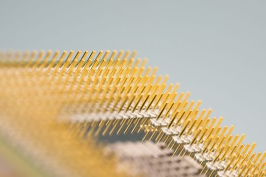
The biggest practical limitation is visibility: most contract manufacturers receive the die and the signed firmware as opaque blobs, and the RTL/IP block list is covered by NDAs, so the "true" software BoM is only available to the silicon vendor's internal security team. Engineering teams have to work from public release notes, microcode update manifests, and the SPDX / CycloneDX files published by the vendor; missing entries should be treated as a supplier-disclosure gap, not a clean bill of health [S1].
Two trackable signals for the next 6 months: (1) wider adoption of CycloneDX-style SBOM attestation by the major x86 and Arm CPU vendors in their public security advisories, and (2) pressure from EU Cyber Resilience Act-style procurement clauses to demand signed microcode manifests at PO time, not at incident time. Both will push the industry to treat the CPU as a tri-part BoM (silicon, package, signed firmware) rather than a single line on a BOM.
For component-level specifications, see shaft key, pressure transmitter, and flow meter.