CPU production today stacks 4 to 16 cores on a single die at TSMC N5/N4 or Intel 7-class nodes, and each finished chip is binned by voltage-frequency behavior before it ships in a specific SKU [S1][S3].
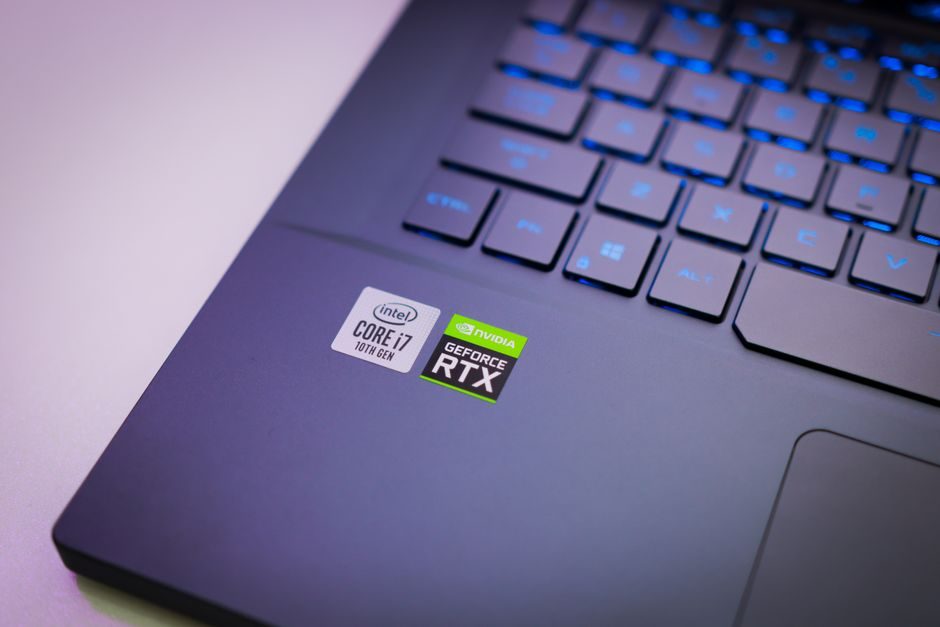
Core count, simultaneous multithreading (SMT, marketed by Intel as Hyper-Threading since 2002) and chiplet-based packaging are now the three knobs that define a CPU's market tier more than gigahertz ever did [S2][S1].
What a "core" actually is on a 2026 die
A CPU core is an independent execution unit with its own integer pipeline, floating-point unit, L1 cache (typically 32 KB I + 32 KB D per core) and private L2 slice, all sharing a larger L3 cache across the die [S1].
Each core also carries an SMT front-end: Intel's Hyper-Threading, introduced on the Xeon line in 2002 and extended across the desktop stack since the Pentium 4 era (800 MHz system bus), exposes one physical core as two logical threads so the pipeline stays fed when one thread stalls on a cache miss [S2].
Process node, transistor density and binning class (e.g., K/KF, X3D, Xeon Silver vs Platinum) are the first things a process engineer checks on a datasheet, because two parts with the same core count can differ 30-50% in sustained all-core boost clocks [S3].
Lithography, FinFET and the yield bottleneck
Current desktop and server CPU dies are fabricated on sub-7 nm FinFET (or GAAFET) processes at TSMC, Intel Foundry and Samsung, with EUV layers inserted at the 7 nm node to print the densest metal and via levels [S1].
Yield is the single biggest cost driver: a wafer that costs on the order of US$15,000-20,000 at 5 nm class can lose 20-40% of dies to defects, and the surviving parts are binned by achievable voltage-frequency corner into different SKUs (the same wafer feeding an i9, an i7 and a Xeon-W SKU is common industry practice) [S1].
For sourcing teams, the practical read is that "node name" alone is not a quality signal; die size, core count, and L3 cache density per mm² move faster than marketing node numbers [S3].
Multi-die and chiplet packaging
High-end CPUs are no longer monolithic: 8-16 core desktop parts and 32-128 core server parts spread compute tiles across multiple chiplets on a single interposer (Intel's "Tile" approach and AMD's "CCD + IOD" layout are the two reference designs) and connect them through a high-speed die-to-die fabric [S1].
For embedded and industrial buyers comparing servo motor drives against an integrated x86 controller, the relevant spec is not "how many cores" but "how many PCIe lanes, how much L3, and what CXL type" the platform exposes, because that is what determines real-time I/O bandwidth [S1].
Hyper-Threading, SMT and the "threads" you actually buy
A 16-core CPU with SMT enabled presents 32 logical processors to the operating system, and on throughput-bound workloads (rendering, compile, AES, video encode) the real gain is typically 15-30% over the same chip with SMT off [S2][S3].
On latency-bound or security-sensitive workloads (certain database locks, side-channel-sensitive crypto, hard-real-time control loops on a PLC) the two virtual threads compete for execution ports, so single-threaded latency can drop and engineers will explicitly disable SMT in BIOS [S2].
Server SKUs historically drop SMT at the top bin (e.g., frequency-optimized Xeon SKUs) to keep per-core turbo stable; this is a process-engineering trade, not a marketing choice [S1].
Selection criteria for industrial / embedded buyers
For an industrial PC, machine-vision station or flow-meter gateway, the four specs that move a procurement decision are: (1) core count vs real-time workload mix, (2) base/boost power envelope (PL1/PL2, TDP), (3) supported memory type and channel count, and (4) long-term-availability / 10-15 year roadmap commitment from the vendor [S3].
Comparison snapshot for typical 2026 industrial CPU options (values are class-typical, not a specific SKU):
- Atom-class / Elkhart Lake refresh: 4-8 cores, 6-12 W TDP, 10+ year availability, soldered BGA, no SMT on the lower bins.
- Core-i class embedded (e.g., Raptor Lake-PS refresh): 8-24 cores, 35-65 W TDP, DDR5 dual-channel, PCIe 5.0 x8 to chipset, 7-10 year availability.
- Xeon-SP scalable (single socket, edge SKU): 8-32 cores, 70-205 W TDP, 8-channel DDR5, PCIe 5.0 x64, ECC mandatory, 5-7 year availability.
- EPYC-edge / SP-class: 16-64 cores, 120-280 W TDP, 12-channel DDR5, CXL 1.1/2.0, 5-7 year availability [S1][S3].
On cost per usable thread, the Atom and Core-i embedded tiers deliver the lowest $/thread at moderate clock; the Xeon tier wins on memory bandwidth and RAS features (ECC, machine-check architecture, lockstep) [S1].
Limits, failure modes and what to watch next
The hard physical limits today are reticle size (around 800-830 mm² per exposure, capping monolithic die area) and thermal density (around 1 W/mm² sustained at the hot spot, above which throttling kicks in) [S1].
The two failure modes that bite embedded integrators are (a) stepping revisions that change the boot firmware expectation (Intel and AMD ship stepping updates mid-cycle, and BIOS/UEFI must follow) and (b) end-of-life on the memory controller side: DDR4 parts are being phased out, and 2026 industrial builds are increasingly DDR5-only, which forces a re-validation of any custom carrier board [S3].
Two trackable signals to monitor over the next 12 months: 18A / 20A node ramp at Intel Foundry (the first GAAFET-class risk production for a high-volume client CPU) and the broader migration of embedded Atom lines onto chiplet packaging, which will change the socket story for long-life industrial designs [S3].
For a current read on the 2026 desktop top-of-stack and how the Intel vs AMD battle maps to those process nodes, the latest ranking round-up is worth cross-checking against your embedded road-map, and on the supply side the semiconductor spot-price index for MOSFET and IGBT gives a useful proxy for the wider fab-utilization picture feeding CPU wafer output.