Flat panel display production has shifted decisively from LCD backplane manufacturing to OLED heterogeneous-material processing, with substrate materials moving from rigid glass to flexible plastics to meet demand for lighter, thinner, foldable end products [S5]. Chinese display panel manufacturers, led by BOE Technology Group, are accelerating OLED capacity expansion across smartphone, tablet, laptop, vehicle-mounted and wearable categories, with public demos continuing at the 2025 Display Innovation China Expo in Shanghai [S6].
The production line itself now revolves around laser patterning and laser cutting of multi-layer organic films, where the tool must hold accuracy and edge quality across stacked layers of differing ablation thresholds [S5]. Buyers specifying equipment in 2026 should plan around the OLED line as the primary roadmap, treat LCD as sustaining legacy, and budget for laser tool flexibility that handles both glass and plastic substrates.
Substrate stack: glass, polyimide, and the move to flexible plastic
Substrate choice drives the rest of the process flow. Rigid OLED lines still run on glass, but the trend is clearly toward flexible plastic — typically polyimide — because it enables thinner panels, smaller bend radii, and roll-to-roll downstream handling [S5]. The trade-off is thermal budget: polyimide cannot take the same high-temperature anneals as glass, so buffer layers and lower-temperature TFT processes (LTPS at reduced peak temperature) become mandatory.
For a buyer evaluating an OLED line, the substrate decision is the first spec cut: glass gives the tightest dimensional tolerance and the highest process temperature window; plastic gives the form factor and weight, at the cost of a tighter thermal envelope and a more demanding laser-cutting step (no cracking, no delamination at the edge). When the same panel plant wants to serve both rigid monitor/OLED-TV builds and foldable phone builds, the laser system has to be reconfigured, not replaced — and that reconfigurability is now a line-tender spec, not a luxury.
OLED vs LCD vs PDP: how the stack differences change the toolchain
LCD cells are passive light modulators sitting on a backlight; PDP cells ionize neon-xenon gas in sub-pixel cavities; OLED cells are self-emissive organic stacks driven directly by the TFT backplane [S3]. That difference cascades into manufacturing. PDP was effectively displaced once LCD and OLED reached comparable color gamut and viewing-angle performance at lower power [S3]. OLED removed the backlight, the diffuser stack, and most of the cell-gap tolerance budget that LCD requires.
In practical production terms: an LCD line is dominated by color-filter lamination, liquid-crystal filling and cell-gap control, with a separate backlight assembly step [S5]; an OLED line is dominated by vacuum thermal evaporation of organic layers, fine metal mask (FMM) alignment for RGB, and encapsulation. The laser patterning step matters most where heterogeneous materials are stacked — i.e., the OLED stack and the touch-sensor integration layer, not the LCD cell itself [S5].
Laser patterning and cutting: the bottleneck of heterogeneous-material processing
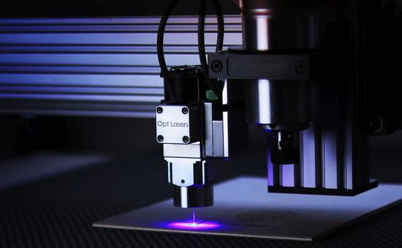
Within an OLED line, the laser system has to pattern and cut layers that are simultaneously organic, metallic and inorganic — each with a different ablation threshold and a different edge-quality requirement [S5]. Edge quality cannot be checked at the end of the line; it has to be controlled in-line, because a single delamination or carbonised edge in a flexible OLED stack kills the fold-life rating.
Three concrete capabilities now define an acceptable laser station: (1) wavelength and pulse-duration tuning per layer so the same beam can ablate an organic emission layer without damaging the metal cathode beneath it; (2) sub-10-micron positional repeatability over a large working area, because the FMM-to-substrate alignment budget is already tight before the laser adds error; (3) stability over sustained duty cycle, since OLED lines run the laser station continuously and downtime directly hits panel yield [S5]. Equipment vendors such as Jiangsu YAWEI-LIS Laser Technology publish their positioning around joint R&D with global display customers and laser-based solutions for the same heterogeneous-material problem [S4].
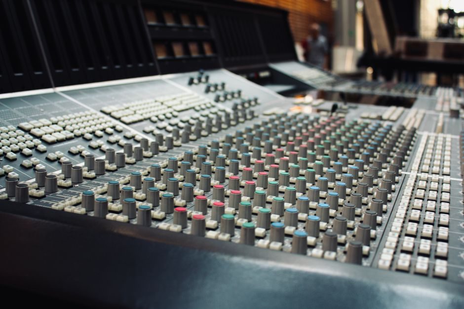
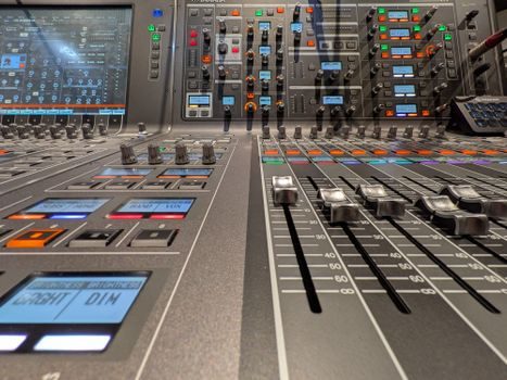
Where the same process knowledge lands in industrial HMIs
The crossover into industrial product categories is direct. An HMI touch panel on a factory floor uses the same TFT backplane, the same cover-glass bonding, and increasingly the same OLED or LTPS-LCD stack as a smartphone — the difference is environmental, not fundamental. Specifiers reading the 2026 HMI Touch Panel Buying Guide should therefore expect display-panel production advances — better touch-sensor integration, narrower bezels, higher luminance OLED — to flow into industrial panels on roughly an 18-to-36 month lag. [S1]
The same substrate shift affects industrial display modules destined for outdoor or in-vehicle use: plastic substrates lower weight, which matters for vehicle-mounted and wearable SKUs, and the laser-cut edge quality directly determines ingress-seal reliability at the bezel. When the procurement team sources both a consumer-grade OLED line and an industrial HMI line, they should audit both vendors on laser edge-quality metrology — the failure modes are identical even though the end products are not.
Selection criteria: matching the production line to the product mix
[S2]
On the same four criteria, the comparison reads as follows. A rigid glass OLED line scores high on tolerance and throughput but loses on form factor; a flexible polyimide OLED line scores high on form factor and weight, and loses on thermal budget and edge-yield; a legacy LCD line scores high on cost-per-panel for monitor and TV sizes and loses on power, contrast and the ability to serve foldable end products. PDP is now a maintenance story for legacy installations and a non-option for new builds [S3]. For plants deciding where to place the next capex, the data point that matters is the OLED line's unit-cost crossover, which is the threshold at which OLED panel production reaches parity with LCD on a per-area basis for monitor sizes — and the public direction of travel from Chinese panel makers is to push that crossover down by adding capacity, not by slowing down [S6].
Standards, sourcing and 2026 sourcing signals to watch
Production-grade OLED and laser-patterning equipment is not governed by a single IEC or ISO display-production standard in the way that, for example, power semiconductor production is anchored to specific device-family standards. What governs the line is the OEM process recipe, the laser's own CE/UL safety certification, and the customer's yield and reliability acceptance criteria. Buyers should therefore audit the equipment vendor on documented process-of-record for the specific stack (RGB OLED versus WOLED, rigid versus flexible) rather than asking for a generic display-production standard. [S3]
Two trackable signals will define the next twelve months. First, the rate at which Chinese panel makers convert LCD lines to OLED lines — BOE's continued investment pace through 2026 is the single most-watched data point for global OLED capacity [S6]. Second, the rate at which laser tool vendors demonstrate in-line edge-quality metrology on flexible polyimide stacks, because that is the metric that currently gates foldable OLED yield and therefore gates the next wave of industrial display and HMI form-factor innovation.
For component-level specifications, see alc panel.