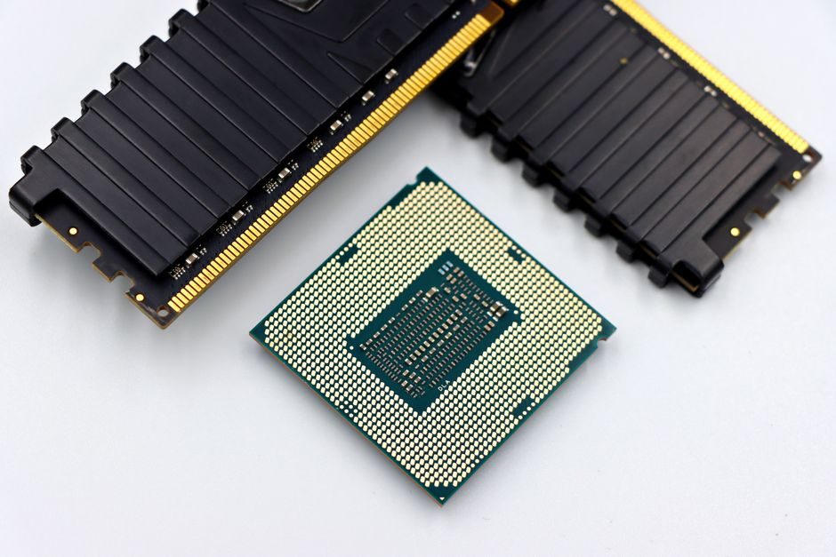
High Bandwidth Memory (HBM) is a JEDEC-standardised stacked-DRAM technology specified in JESD238, with the current shipping generation reaching HBM3E and engineering samples of HBM4 demonstrated in 2025–2026 [S4]. Only three IDM memory manufacturers qualify as primary HBM suppliers: SK hynix, Samsung Electronics, and Micron Technology — no second-source foundry exists for the DRAM die, the TSV (through-silicon-via) process, or the stacked-die assembly [S4].
The HBM supply chain is therefore a three-vendor oligopoly, and HBM cannot be substituted by pressure transmitter-style commodity sourcing; qualification cycles run 12–18 months because the HBM base die must be matched to a specific logic process node (typically 5 nm, 4 nm, or 3 nm) for the customer's ASIC or GPU. This article maps vendor positioning, spec boundaries, and the engineering criteria a spec-driven buyer should use to evaluate HBM offers.
JEDEC standard scope: what HBM is and is not
HBM is defined by JEDEC JESD238 (HBM) and its successor JESD238A (HBM2), with HBM3 specified separately and HBM3E / HBM4 tracked under follow-up JEDEC publications [S4]. HBM uses a wide-interface parallel bus (1024-bit per stack in HBM2/HBM3) over a silicon interposer, giving per-pin bandwidth far above DDR5's 64-bit channel and far above GDDR6X's 16-bit/pin PAM4 signalling [S4].
HBM is NOT a drop-in for flow meter-style standard instruments: every HBM stack is custom-binned to a specific host die, so two GPUs from the same vendor can use different HBM SKUs. HBM is also not compatible with HMC (Hybrid Memory Cube, Micron/Hynix legacy standard) or with any 2.5D/3D memory using active interposers — HBM is a passive-interposer, TSV-stacked, JEDEC-only standard [S3][S4].
Vendor tier map: SK hynix, Samsung, Micron
SK hynix has been the volume leader in HBM3 and HBM3E from 2024 through 2026, holding the largest share of NVIDIA H100/H200 and AMD MI300X allocations and the dominant share of HBM3E 8-Hi / 12-Hi stacks [S4]. Samsung has qualified HBM2E and HBM3 at lower volumes and has been working to qualify HBM3E with NVIDIA's 2025–2026 generation accelerators; Samsung's pitch is advanced-NAND-like thermal performance via its proprietary MR-MUF (mass reflow moulded under-fill) process [S4].
Micron entered HBM late but qualified HBM3E on its 1β (1-beta) DRAM node, with volume ramp on NVIDIA Blackwell B100/B200 platforms announced for the 2025–2026 window [S4]. The relevant comparison on three decision criteria:
SK hynix vs Samsung vs Micron on HBM3E: capacity-per-stack (24 GB 8-Hi vs 24 GB 8-Hi vs 24 GB 8-Hi), thermal solution (TC-NCF vs MR-MUF vs TC-NCF), and volume ramp (lead vs 1–2 quarters behind vs 1–2 quarters behind). All three meet JEDEC JESD238 pinout and timing, but lead-time and binning quality still differ by vendor [S4].
Spec boundaries buyers must verify
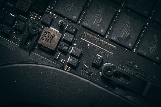
Stack height: HBM3E 8-Hi stacks are typically 720–775 µm total height depending on TSV pitch and base-die thickness, and 12-Hi stacks reach ~900 µm; this drives the maximum package z-height that the host ASIC package substrate must accommodate [S4]. Die density: 16 Gb, 24 Gb, and 32 Gb per die are qualified by the three vendors across HBM2E, HBM3, and HBM3E respectively, giving 16 GB / 24 GB / 32 GB per 8-Hi stack and 24 GB / 36 GB / 48 GB per 12-Hi stack [S4].
Bandwidth: HBM3E per-pin data rate is 9.6 Gb/s in the JEDEC baseline (9.6 Gbps × 1024-bit = ~1.2 TB/s per stack), with vendor-extended parts reaching 9.8–10.0 Gb/s in binned SKUs [S4]. Power: HBM stacks operate at 1.2 V VDD and 0.9 V VDDQ, with total stack power (read/write) in the 5–8 W range depending on utilisation; full-reticle HBM subsystems (4–8 stacks) on a GPU pull 25–50 W from the memory subsystem alone [S4].
Who HBM is for, and who it is not for
HBM is FOR: AI training accelerators (NVIDIA, AMD, custom ASICs), high-end FPGA compute cards, and high-throughput network processors where per-package bandwidth >1 TB/s is mandatory and the host can pay the PCB / interposer / thermal cost. HBM is NOT for: cost-sensitive edge AI inferencing, consumer graphics, embedded controllers, or any industrial valve-class cost-driven application — these use LPDDR5X, DDR5, or GDDR7 instead [S4].
Buyers who only need 50–200 GB/s of memory bandwidth (typical for industrial controllers, PLCs, and servo drives) should spec DDR5 or LPDDR5X, not HBM. A PLC running ladder logic on 10 ms scan times needs neither the bandwidth nor the thermal envelope; the relevant servo motor feedback loop similarly runs fine on DDR4-class memory.
Qualification flow and lead-time
Typical HBM qualification cycle: 12–18 months from NDA + initial sample to qualified-mass-production (QMP), with three milestones — engineering sample (ES), qualification sample (QS), and production sample (PS). Each milestone requires the host ASIC to re-tapeout its PHY and re-validate the interposer routing because HBM signal-integrity is sensitive to interposer micro-bump pitch (typically 55–65 µm) and TSV pitch (typically 6–10 µm) [S4].
For the upcoming HBM4 generation (JEDEC under definition, vendor demos in 2025–2026), lead-times are expected to extend further because HBM4 widens the interface beyond 1024 bits per stack and uses a custom base die in some vendor roadmaps, which removes the cross-vendor PHY compatibility that HBM3E retains [S4].
Standards and what to cite in a spec sheet
For an OEM datasheet, the citable standards are: JEDEC JESD238 (HBM base), JEDEC JESD238A (HBM2), JEDEC HBM3 (JESD238B-equivalent publication), and per-vendor HBM3E product briefs [S3][S4]. For thermal and reliability, JEDEC JESD22-A104 (temperature cycling) and JESD22-A110 (HTOL) are the typical qualification references, though HBM-specific thermal-via under-fill testing is vendor-proprietary [S3].
Buyers should never specify a non-JEDEC HBM variant (HMC, HBM-PIM, or vendor-private extensions) without an explicit waiver, because the 1024-bit interface, pseudo-channel mapping, and refresh behaviour are JEDEC-defined only [S4]. For the upstream supply chain (wafer foundry, TSV process, stacked-die assembly) the relevant upstream/downstream map is detailed in HBM Memory Upstream and Downstream: Spec Map, Capacity Tiers, and SiP Sourcing [S3].
Next, the Advanced Chip Packaging Supply Risk: 2026 Substrate Bottleneck Map page covers the 2.5D / 3D interposer substrate capacity that constrains HBM shipments. Trackable signals for the next 6 months: SK hynix HBM3E 12-Hi 36 GB qualification, Micron HBM3E 32 Gb die on 1γ node, and JEDEC publication of the HBM4 baseline (timing undefined as of 2026-07) [S4].