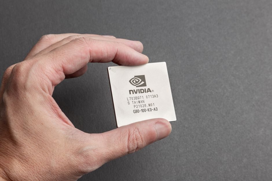
A leading-edge AI GPU in 2026 is a multi-die package: one compute die fabricated on a 5 nm or 3 nm FinFET process, surrounded by 4 to 8 HBM3/HBM3e memory stacks mounted on a 2.5-D silicon interposer, with the whole assembly sealed in an organic-substrate BGA [S1].
That packaging shift is the real production story — the HBM stack capacity, the interposer area, and the CoWoS-S/CoWoS-L throughput at TSMC now gate the AI accelerator supply chain more than the raw compute-die yield, and frame why GPU production technology: process families, materials and selection reads as a node-and-yield problem rather than a transistor problem [S1].
Compute-die process nodes and the FinFET-to-GAA transition
TSMC's N5 (5 nm FinFET) and N3 (3 nm FinFET) nodes are the workhorse processes for the 2024–2025 generation of data-centre GPUs, with N3E and N3P variants used for higher-volume SKUs and N3X reserved for the highest-Vcore parts [S1]. N4 (4 nm) is essentially a 5 nm optical shrink with new SCAR (Self-Aligned Cell on Recessed layer) rules and ships in 2022–2024 gaming and mid-range accelerators [S1].
Samsung Foundry's 4 nm GAA (gate-all-around, MBCFET) process entered production in 2022 and is used for selected consumer and mobile GPUs; the transition to a true GAA ribbon FET for high-volume data-centre GPUs is staged for the 2 nm node, where Samsung SF2, TSMC N2, and Intel 18A all move to a nanosheet GAA architecture [S2]. Each GAA generation delivers roughly 25–30% lower power at iso-performance or 10–15% higher performance at iso-power versus the prior FinFET node, with the exact split depending on standard-cell library and SRAM bitcell used [S1].
Wafer fabrication, EUV, and the reticle limit
All three leading-edge nodes (TSMC N3, Samsung 4LPP/3GAP, Intel 4/3) require EUV lithography at 13.5 nm wavelength — TSMC's N7+ (2019) was the first high-volume FinFET to insert EUV, and every node since has increased the number of EUV layers until, on N3, the majority of the critical front-end layers are EUV-patterned [S1]. ASML's NXE:3800E and the higher-NA EUV EXE:5000 systems are the only production tools; high-NA EUV is used for the most aggressive via and contact layers on 2 nm-class processes because the 8 nm resolution halves the number of multi-patterning steps required [S1].
The reticle limit drives packaging decisions before the wafer decision: a 33 mm × 26 mm maximum reticle field on EUV tools caps a single-die GPU at roughly ~800 mm², and a reticle-stitched multi-die reticle (e.g. Cerebras wafer-scale, Tesla Dojo) is the way around it — that is why the highest-end AI GPUs are now chiplets rather than monolithic dies [S1][S2].
2.5-D CoWoS interposer, HBM3e, and the bandwidth wall
High-bandwidth memory (HBM) is the second die-level decision and the real production bottleneck in 2025–2026. An HBM3e stack is built on a separate wafer — typically a 12-inch (300 mm) DRAM wafer from SK hynix, Samsung, or Micron — with 8 to 12 dies vertically stacked using through-silicon vias (TSV) bonded with microbumps, then diced and placed on a passive silicon interposer alongside the compute die via TSMC's CoWoS-S (silicon interposer) or CoWoS-L (RDL fan-out with local silicon bridges) flow [S1].
Six or eight HBM3e stacks around a single GPU deliver roughly 1.5 TB/s to 1.8 TB/s of memory bandwidth, with HBM4 (planned ramp 2026–2027) targeting 3 TB/s+ on wider 2048-bit interfaces — the same constraint that has made Top Connector Companies 2026 read as a high-speed signal-integrity story rather than a connector-pin-count story [S1][S2].
Substrate, PCB, and board-level assembly
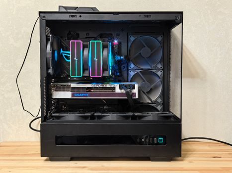
The CoWoS package is mounted on an organic flip-chip BGA substrate (typically Ajinomoto build-up film, ABF, dielectric layers stacked with 2-µm-class L/S lithography), which itself sits on a server-class PCB carrying 24 to 32-layer stack-ups, 85 Ω differential pairs for PCIe Gen5/Gen6, and 1.5 oz copper power planes for the 600 W to 1000 W TDP envelope of a top-bin AI GPU [S1][S2].
Thermal headroom is the third design axis: a 700 W class GPU board needs a cold-plate plus 65–70 °C water-loop coolant or an equivalent two-phase immersion/evaporative loop, with the GPU's reliability screen rated for 95 °C junction under sustained workload and a 105 °C Tjmax [S2]. This is where Air Compressor Production Technology overlaps the AI build-out — plant spec teams that pair compute and process-cooling now spec the same copper-loop standard [S1].
Interconnect: NVLink, PCIe Gen5/Gen6, and the host link
Inside a server, GPUs talk to the host CPU over PCIe Gen5 ×16 (64 GB/s) or PCIe Gen6 ×16 (128 GB/s, on the 2025–2026 ramp), and to each other over Nvidia's NVLink — the 4th-generation NVLink used in H100-class parts provides 900 GB/s of aggregate GPU-to-GPU bandwidth, and the 5th-generation NVLink shipped in 2024–2025 raises that to ~1.8 TB/s [S1].
For non-Nvidia fabrics, AMD's Infinity Fabric and Intel's Xe Link play the same role, while the Open Compute Project (OCP) is standardising UBB (universal baseboard) and OAM (OCP Accelerator Module) form factors so a single 1U/2U sled can host eight GPUs on a common mezzanine — the spec work that has made Connector Production Technology increasingly read as a mezzanine-and-rail story [S1][S2].
Packaging comparisons: monolithic vs chiplet vs 3-D
Three packaging options now compete for AI accelerator production. Monolithic reticle-size dies (≤ ~800 mm² on N3) are simplest but cap the die area; chiplets on an interposer or RDL fan-out (e.g. AMD CDNA 3 / MI300 family on CoWoS-S) scale to >1000 mm² of effective silicon with a 2 TB/s HBM3e envelope; and full 3-D stacked logic-on-logic (e.g. SRAM cache dies bonded face-to-face) is the route to 2 TB+ on-die cache and is being prototyped on TSMC SoIC-X [S1].
The decision rule for process engineers: monolithic when the design fits one reticle and you can yield >70% known-good-die; chiplet (CoWoS-S) when compute and I/O scale differently and you want to mix nodes (e.g. 5 nm compute + 7 nm I/O); 3-D SoIC when memory bandwidth per compute die is the binding constraint and you can absorb the extra thermal density [S1][S2].
The two cost-driven signals worth watching in late 2026 are HBM3e allocation at the four major suppliers and TSMC's CoWoS-S/CoWoS-L monthly wafer-out, since both gate finished-goods supply more than the leading-edge compute-die yield — a spec the same way the offshore-wind pipeline is gated by Offshore wind 2026: market size, sub-segments and the install window, not by single-turbine cost.
For component-level specifications, see pressure transmitter, flow meter, and industrial valve.