A complete LED device is the sum of four coupled process chains: epitaxial growth of GaN/InGaN multi-quantum-well structures on 2- to 6-inch sapphire or SiC substrates, chip-level semiconductor processing, phosphor-conversion packaging, and secondary optical lens moulding [S2].
White-light LED packages in volume production combine a blue GaN die (dominant wavelength 440-470 nm) with a cerium-doped YAG:Ce or nitride phosphor layer, with correlated colour temperatures typically engineered across 2700-6500 K for general-lighting SKUs [S1]. Secondary optics are then moulded as 3-160° beam-spread PMMA or silicone lenses to deliver the luminaire-level distribution [S1].
Substrate Selection and Epitaxial Growth Windows
Patterned sapphire substrates (PSS) dominate mid-volume GaN LED lines because the cone-patterned surface reduces threading dislocation density in the over-grown GaN layer, lifting internal quantum efficiency versus planar sapphire at the same drive current [S2]. SiC substrates are used where vertical-current spreading and lower thermal resistance outweigh substrate cost; Si substrates remain a cost-driven option for mid-power consumer-indicator SKUs but with trade-offs in lattice-mismatch-driven efficiency.
Metal-organic chemical vapour deposition (MOCVD) reactor temperatures for the GaN buffer, n-GaN, MQW active region, and p-GaN layers sit broadly in the 700-1100°C window, with the InGaN well typically grown cooler (around 700-850°C) to suppress indium desorption. VTE (vacuum thermal evaporation) is the parallel dry-process route used for OLED lighting panel stacks, where organic small-molecule layers are deposited sequentially without breaking vacuum to avoid interface contamination [S2]. A v-process line configured for OLED stack deposition typically holds base pressure below 10^-6 mbar to keep the organic-interface water-vapour budget within the encapsulation spec.
Front-End Fab: Lithography, Etch, and Metallisation
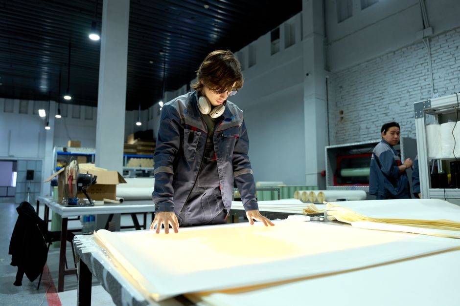
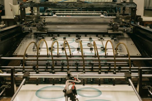
Front-end LED processing follows a standard compound-semiconductor flow: photolithography defines the mesa, then inductively coupled plasma (ICP) dry etching with Cl-based chemistries cuts through the p-GaN / MQW / n-GaN stack to expose the n-contact layer. Etch depths are typically sub-2 µm, and sidewall damage control is critical because plasma-induced defects act as non-radiative recombination centres that pull wall-plug efficiency down. RF power, gas-flow and chamber-pressure trim on the etch tool is typically verified against a multifunction process calibrator before each cassette run. [S1]
The OLED equivalent uses low-work-function cathodes (Mg:Ag, LiF/Al) capped by a thin metal encapsulation [S2].
Phosphor Conversion and White-Light Assembly
White LED assembly combines the blue (or royal-blue) die with a phosphor layer, almost always cerium-doped yttrium aluminium garnet (Y3Al5O12:Ce) for cool-white or a mix of YAG:Ce plus red nitride (CaAlSiN3:Eu2+) for high-CRI warm-white. The phosphor is dispersed in a silicone encapsulant (typically methyl-phenyl silicone) and either dispensed as a dome over the die or pre-moulded as a remote-phosphor plate above the cavity. [S2]
Remote-phosphor architectures lower phosphor operating temperature by 20-40°C versus conformal coating, which slows silicone yellowing and lumen-maintenance drift, a key spec lever for industrial buyers writing lumen-maintenance contracts (L70/B50 or L90/B10 over 50 000 h). The encapsulant cure step runs 150-180°C for 1-4 hours, and the package substrate is almost always an FR-4 or aluminium-core MCPCB carrying the lead-frame and bond wires.
Secondary Optics: Beam Shaping 3° to 160°
Secondary optical design is specified as a 3-160° beam-angle range, with the actual part geometry chosen to support the luminaire's photometric target — narrow 3-10° for spot, 24-45° for downlight, 60-90° for area, and 120-160° for diffuser or street-lighting distributions [S1]. Lenses are typically injection-moulded PMMA (UV-stable grades) or high-temperature silicone for high-flux COB (chip-on-board) packages where the phosphor-side operating temperature can exceed the PMMA glass-transition point.
Optical-design software in vendor flows couples ray-tracing (Monte-Carlo, 1-10 million rays) with the LED source model, and tolerancing is set against the luminaire's IES file target rather than the bare-LED distribution. For industrial buyers evaluating flow-meter or pressure-transmitter projects on the same line, the same optical-tolerancing discipline (ray-count, source-model fidelity, ±0.05 mm mould tolerance) is the relevant comparison point.
Process Comparison Across the Three Main LED Families
Selection of LED type maps directly to the process chain that follows, and the four criteria below are the ones a process engineer or sourcing manager should pin down before writing a tooling PO. [S3]
Criteria A — substrate and MOCVD window: GaN-on-sapphire is the volume default; GaN-on-SiC trades cost for thermal performance; GaN-on-Si is the cost-down option with efficiency penalty. OLED uses glass or flexible PI substrates at room-temperature VTE deposition [S2].
Criteria B — colour-conversion method: inorganic LED relies on phosphor-in-silicone or remote phosphor; µLED and mini-LED skip phosphor and use colour filters or quantum-dot enhancement films (QDEF); OLED generates white either by tandem blue+yellow emitters or by RGB side-by-side sub-pixels.
Criteria C — driver and control: LED is constant-current driven at 350 mA-1.5 A per die (or 150-700 mA for mid-power 5630/3030 packages), with dimming by PWM, CCR, or 0-10 V analogue; OLED is voltage-driven (typically 3-15 V stack) with current-limiting drivers.
Yield, Reliability, and Standards Anchors
Reliability specs are written against LM-80 (lumen maintenance over 6 000-10 000 h with projection to 50 000 h), TM-21 (the projection algorithm), and IEC 62471 (photobiological safety — risk-group classification). Process-side, the dominant yield loss modes are electrostatic-discharge damage at die-attach, silicone-delamination at the phosphor-dome interface, and bond-wire fatigue under thermal cycling; these are screened out at the LED-binning stage (typically 3- or 5-step MacAdam ellipses for colour and ±5% flux bins). [S1]
Buyer-Side Process Levers in 2026
Three levers are visible in the 2025-2026 OEM guidance: first, transition from conformal phosphor to remote-phosphor plate for L90/B10 commercial-flux programs; second, tighter MacAdam ellipse bins (3-step) for premium architectural SKUs; third, audit of MOCVD recipe (V/III ratio, growth pressure around 200-400 mbar, carrier-gas H2/N2 split) to lock IQE at a given drive-current density. The same SQC discipline (Cp, Cpk on flux and Vf at probe-test) governs throughput-yield on BESS pack lines, as covered in the BESS manufacturing process reference. [S2]
Process engineers cross-spec'ing LED fixtures with smart-manufacturing lines should review the EV charger smart manufacturing automation stack for trace-and-yield patterns; the automation, MES hooks and quality-gate logic carry over directly into a 2026 LED-pack line.
Watch for vendor technical-data-sheet revisions citing LM-84 (luminaire lifetime) projected to L90 in place of L70 as the new commercial baseline.