PCB smart manufacturing in 2026 is defined by the convergence of high-speed surface-mount technology (SMT) lines, machine-vision automated optical inspection (AOI), and closed-loop Manufacturing Execution Systems (MES) wired into the enterprise resource planning (ERP) layer — replacing the discrete, paper-ticket workflow that still dominates mid-tier EMS shops [S2].
One-stop EMS providers operating since 2008 (LST, 18 years tenure as of 2026-06) now bundle component procurement, PCB design, prototyping, SMT assembly, and in-circuit / flying-probe testing under a single MES instance, with the customer-facing order tracking dashboard driven off the same database the shop floor uses [S3]. Sierra Circuits and LST both run ISO 9001:2015-certified quality systems and expose real-time WIP, yield, and cycle-time data to OEM customers [S3][S5].
Core Process Stack: Solder Paste, Pick-and-Place, Reflow, AOI, ICT
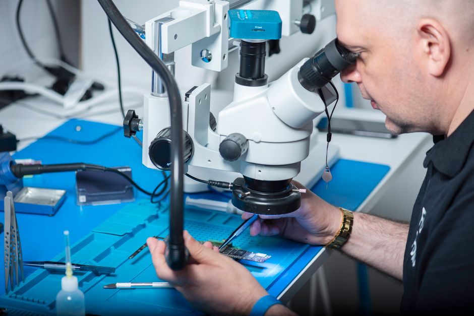
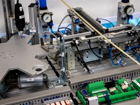
The canonical PCB smart-manufacturing line in 2026 runs solder-paste stencil print → 3D SPI (solder paste inspection) → high-speed chip shooter + flexible placer → forced-convection reflow oven with nitrogen option → 3D AOI → in-circuit test (bed-of-nails or flying probe) → functional test → conformal coating or underfill where required [S2][S3].
Modern pick-and-place platforms are specified for placement rates in the 60,000–150,000 CPH range, component envelopes from 01005 (0402 metric) up to large BGAs and odd-form connectors, and ±25 µm placement accuracy at 3-sigma — these are the published OEM datasheet bands that procurement engineers cross-check against IPC-9850-equivalent throughput claims [S3]. Reflow profiles are now stored per-pallet in the MES and replayed on each board for full traceability, with profile-control software logging preheat, soak, TAL (time above liquidus, typically 30–90 s for SAC305 lead-free), and peak temperature (235–250 °C for lead-free) per board serial [S2].
MES / ERP Integration and the IPC Quality Anchor
The "smart" in PCB smart manufacturing sits on three data fabrics: MES for shop-floor execution, ERP for BOM and cost roll-up, and a Quality Management System (QMS) that owns the IPC class declaration per assembly [S1][S2].
Acceptance criteria are anchored to IPC-A-610 for assembled boards and IPC-6012 for bare-board fabrication, with Class 2 (dedicated service electronics — consumer, industrial) and Class 3 (high-performance / harsh environment — automotive, aerospace, medical) dictating the AOI sampling rate, X-ray coverage for BGA/QFN hidden joints, and rework allowance [S3]. ISO 9001:2015 plus, where automotive or medical work is on the line, IATF 16949 or ISO 13485, sit one layer above the IPC spec and are audited annually [S3][S4]. A typical 2026 EMS audit pack cross-references the IPC class, the ISO standard, the customer-specific build standard (e.g. CID+ certified designers), and the MES yield dashboard, all keyed by the board serial [S2][S3].
Selection Criteria: When Smart-Factory EMS Beats Captive Lines
Smart-manufacturing EMS outsourcing makes sense when the OEM needs low-to-mid volume (under ~50,000 assemblies/yr per part number), design-iteration velocity, and shared capex on SMT + AOI + X-ray — captive lines pay back only above that band and only when the BOM is stable for 3+ years [S2][S3].
For high-mix, low-volume work (IoT, smart-home gateways, sensor edge nodes) where NPI cycles run in days rather than quarters, a smart EMS with on-shore quickturn and a digital thread from Gerber/ODB++ to AOI is the lower-risk path — the same MES the EMS uses to control its own lines will push the OEM's design rules (component keep-out, paste aperture ratio, fiducial placement) back into the DFM review at quote time [S1][S5]. The same MES-anchored DFM loop is also what makes smart camera and smart meter OEMs — both of which build on EMS-supplied PCBA — possible to iterate on a 4-week cadence rather than a 4-quarter cadence [S5].
Decision Frame: 2026 EMS Provider Tiering
Three tiers dominate 2026 EMS sourcing: (a) global tier-1 with multi-site capacity and proprietary execution software (the GMS model — Fortune-customer telecom and networking focus, operating since 2008) [S2]; (b) mid-tier one-stop shops with 18+ years of PCB+PCBA integration, ISO 9001:2015 quality systems, and a public online quoting engine that ties Gerber upload to DFM feedback in minutes (LST, 2008–2026) [S3]; and (c) trading-platform aggregators (made-in-china.com factory listings) where ISO 9001:2015, ISO 45001:2018 OHSMS, and revenue band (USD 1–10 M annual) are buyer-disclosed audit fields [S4].
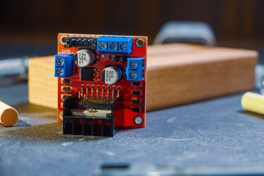
Cost-per-joint in 2026 still moves with panel utilization, stencil-step count, and component mix — a 4-layer ENIG 1.6 mm FR-4 board with 0201 passives and one BGA commonly lands in the USD 0.20–0.50 per joint range for low-volume runs, with setup/NRE and stencil cost amortized across the lot size [S3][S4]. Lead time from Gerber release to first-article shipment is 5–10 working days for smart-EMS quickturn, and 3–4 weeks for volume [S3]. Where factory-floor material handling itself is a design constraint — heavy copper busbars, large-format substrates — the same MES-driven line control logic now also runs in adjacent metals and aluminum smart manufacturing cells, and the lessons transfer directly.
Smart-Home and IoT PCB Assembly: A 2026 Use-Case Slice
Smart-home and home-automation PCBA work has its own assembly profile in 2026: Wi-Fi/BLE modules (typically 30 × 16 mm SiP or castellated module on a 2- or 4-layer FR-4 carrier), AC-DC or DC-DC converter sub-sections, antenna keep-out enforced via DFM, and a final 3D AOI plus flying-probe test at the gateway PCB level [S5].
Designers targeting this segment must keep the module antenna clearance (typically 5 mm of all copper and components, per the SiP datasheet) clear of the SMT placement field, which is one of the most common DFM rejects a smart EMS will flag before stencil print [S5]. The downstream shipping data from this segment is what drives investment in line-side additive manufacturing material for fixturing and jigs — printing AOI nests, selective-coating masks, and ICT fixtures in PA12 or ABS on the shop floor cuts lead time on a new SKU from 5 days to 5 hours.
Limits, Failure Modes and What Smart PCB Lines Cannot Fix
Smart PCB manufacturing does not recover from a bad stackup, a wrong impedance target in the Gerber, or a BOM line pointing at an NRND component — MES and AOI only execute, they do not design [S1][S2].
Three failure modes dominate 2026 EMS returns: (1) BGA head-in-pillow / non-wet joints caught only by X-ray because AOI is a top-down view, which is why smart lines for Class 3 include 100 % X-ray on BGA/QFN and AOI on everything else; (2) tombstoning of 0201 / 01005 passives from paste-volume imbalance, which 3D SPI catches at the first step before reflow; (3) counterfeit or refurbished components slipping through when the BOM sourcing happens outside the EMS's approved-vendor list, which is the reason the smart-EMS contract scopes the AVL inside the MES, not in a side spreadsheet [S2][S3]. Specifying an EMS that owns the BOM sourcing under its ISO 9001:2015 QMS is the single most effective way to close the counterfeit loop, and it is now standard language in EMS MSAs [S3][S4].