
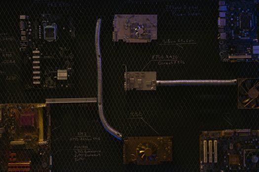
Power semiconductor manufacturing converts a 150 mm, 200 mm, or 300 mm silicon wafer into discrete MOSFETs, IGBTs, Schottky diodes, and wide-bandgap SiC/GaN devices through a fixed sequence of thermal, lithographic, etch, implant, dielectric, and metallisation steps [S3].
The line is the same regardless of whether the end device is a 12 V logic MOSFET, a 6.5 kV IGBT module, or a 1200 V SiC planar MOSFET; what changes is the doping profile, the active-area termination, and the back-side metallurgy, not the unit-process sequence [S3]. Three process nodes define the leading-edge logic/speciality-fab baseline that 2026 power-discrete and IC lines are built around: Intel 18A (1.8 nm-class, RibbonFET gate-all-around + PowerVia back-side power), Intel 3 (3 nm-class, FinFET), and Intel 16 (22 nm-class, FinFET, mature for analogue/mixed-signal and embedded power management) [S1].
Wafer Front-End: Crystal Growth, Epitaxy, and Cleanroom Substrate
Czochralski-grown mono-crystalline silicon ingots are sliced into prime wafers, then a homo-epitaxial Si layer or a hetero-epitaxial SiC/GaN layer is grown on the polished substrate to set the breakdown voltage, on-resistance RDS(on), and leakage floor of the finished die [S4]. SiC epitaxial wafer market reporting (2024-2030 horizon) tracks 150 mm and the ongoing 200 mm SiC epi transition that reduces die cost by roughly 1.5-1.8x per wafer area at the same thickness tolerance [S4].
Epitaxial reactor throughput, measured in wafers-per-hour and micrometres-per-hour growth rate, is the single biggest capex lever between a 1200 V SiC MOSFET line and a 650 V GaN-on-Si line; the 2024-2030 epi market report tracks these KPIs alongside defect density (BPD/cm² for SiC, threading dislocation density for GaN-on-Si) as the primary yield gates [S4]. For SiC, basal plane dislocation density below 1 cm⁻² is the working target for 1200 V MOSFETs; GaN-on-Si lines tolerate higher dislocation density but pin device Rdson to the Si substrate thermal budget [S4].
Thermal Oxidation, Implant, and Dopant Activation
Gate-oxide growth on Si runs in a vertical or horizontal furnace at 850-1100 °C in dry O₂ or wet O₂; for 1200 V SiC the gate dielectric is a deposited SiO₂ annealed at 1250-1350 °C in NO or N₂O to passivate interface traps and stabilise threshold voltage [S3]. Ion implantation dials source/drain, body, and JFET region doping; activation anneals differ sharply by material: Si uses 1000-1100 °C spike or soak anneal, SiC needs 1600-1700 °C activation because of the low dopant solid solubility, and GaN-on-Si is not implanted at all — the 2DEG forms spontaneously at the AlGaN/GaN heterojunction [S3].
For power lines, the thermal budget of activation drives the choice of metallisation: SiC lines run Al/Si or Al/Si/Cu top-side with Ni/Ag or Ti/Ni/Ag back-side, with anneal steps kept below 500 °C to avoid reaction between the ohmic contact and the SiC substrate [S3]. Foundries running Intel 3 and Intel 16 processes use a much wider thermal envelope for interconnect, but Intel 18A's PowerVia back-side power delivery removes the need for global routing on the device layer and is the reason 1.8 nm-class logic can hit the density-per-watt that 2026 power-management ICs benchmark against [S1].
Lithography, Etch, and Planar vs Trench vs Fin Architecture
Stepper resolution (KrF 248 nm, ArF 193 nm dry, ArF 193 nm immersion) sets the minimum cell pitch for planar power MOSFETs, which typically run 0.18-0.5 µm lithography for the active area and 0.35-0.5 µm for the termination [S3]. Below 100 V, Trench MOSFETs (deep Si etch, aspect ratio 10:1 to 30:1) replace planar to cut RDS(on) per cell; above 600 V, the dominant architecture is still planar or slight-trench, because deep trenches on SiC drive up epitaxial cost without proportional RDS(on) gain [S3].
Intel 18A switches the gate from FinFET to RibbonFET (gate-all-around, with stacked Si nanosheets), which gives better short-channel control at sub-1.8 nm gate length; this architecture is not yet used for discrete power devices, but it defines the mixed-signal/power-management IC reference flow that 2026 PMIC designs are scaled into [S1]. Intel 3 keeps FinFET for higher drive current at the cost of more leakage; Intel 16, at 22 nm-class, is the analogue/embedded-PMIC workhorse for fabless power companies that need bipolar-CMOS-DMOS (BCD) on a single die [S1].
Dielectrics, Metallisation, CMP, and Back-Side Process
Inter-layer dielectric (ILD) is usually a high-density-plasma or PECVD SiO₂; for 1200 V SiC lines, a benzocyclobutene or polyimide overcoat is added to handle the high dV/dt edge rates that would otherwise crack a SiO₂ passivation [S3].
Back-side grinding thins the wafer to 100-200 µm for Si power discretes and as low as 50-100 µm for thin-package GaN-on-Si; SiC is typically left thicker (350-500 µm) because of mechanical fragility, and a back-side implant + laser anneal forms the back-side ohmic contact [S3]. For PowerVia-based 18A logic, the wafer is bonded to a carrier, the Si substrate is removed down to the buried power rail, and a Cu back-side power network is plated — this is the only production 2026 node that flips the conventional front-side-only metallisation rule [S1].
Dicing, Die Attach, and Packaging
Dicing options are blade saw (industry default), laser grooving + blade break, and plasma dicing (stealth dicing); SiC uses laser + blade to avoid chipping, and GaN-on-Si uses plasma dicing to avoid back-side metal peel [S3]. Die-attach options scale with the thermal budget: solder (SAC305, SnAg, AuSn for high-temperature SiC), silver sinter paste (300-400 °C, 200-300 W/m·K bond-line thermal conductivity, dominant in EV traction inverters), and conductive epoxy for low-cost consumer lines [S3].
For wide-bandgap modules, Al bond wires are increasingly replaced by Cu clips to lower parasitic inductance and survive 50-200 A/cm² continuous current at the dV/dt edges of a SiC switching node [S3].
Yield, Test, and Process-Engineer KPIs
Power-line yield is tracked on three axes: wafer-sort yield (parametric pass at probe), final-test yield (function + RDS(on) + Vth + BV distribution), and burn-in yield (early-life failure rate, expressed in DPPM) [S3]. A 2026 process-engineer audit compares the Intel logic/foundry baseline (Intel 18A / Intel 3 / Intel 16) against a discrete power baseline (180 nm planar or 110 nm trench BCD) on five decision criteria: lithography node, dielectric stack, back-side process, contact metallisation, and packaging — Intel 18A wins on lithography node and back-side process (PowerVia), while 180 nm BCD wins on dielectric thickness, cost-per-die, and high-voltage termination headroom [S1].
For a process engineer choosing a foundry partner for a power management IC in 2026, the gating question is whether the die needs >700 V isolation (stay on ≥110 nm BCD, use SiC epi as needed) or <100 V logic-integrated power (use Intel 3 or Intel 16 with embedded BCD) — these are the two design points Intel's March 2026 process roadmap explicitly covers [S1]. The power cable analogy is intentional: voltage class and current density drive the conductor cross-section, just as breakdown voltage and RDS(on) drive the active-area design rules in a power die.
Standards, Sourcing, and Where the 2026 Line Diverges

Process-engineer sourcing pulls from three buckets: Si-line equipment (Applied Materials, Lam, TEL, ASML), SiC bulk + epi suppliers (Wolfspeed, II-VI/Coherent, ROHM/SiCrystal, SK Siltron CSS), and analytics/yield software (PDF Solutions Exensio + Sapience lines, with a 2026 release centred on multi-vendor in-line data fusion) [S2]. Epitaxial wafer market data points to 200 mm SiC epi as the structural shift between 2024 and 2030, with cost-per-die and BPD/cm² as the two published KPIs [S4].
Advanced analytics for power lines (PDF Solutions' June 2026 release) is built around the same Exensio platform used for foundry-logic yield — the practical effect is that a 2026 power fab now runs commonality-aware FDC (fault detection and classification) across implant, etch, CMP, and back-side grind, instead of separate SPC charts per tool [S2]. For engineers also tracking other 2026 line changes, the additive manufacturing material reference is a useful parallel on powder-to-part yield, and the power meter page covers the end-of-line electrical test gear that a power fab's final-test cell bolts into.
For a related factory-floor data view, this nickel smart manufacturing 2026 spec snapshot covers the in-line analytics pattern that a power fab can port into its etch and CMP cells, while the MEMS sensors in smart manufacturing 2026 reference maps the same KPI logic onto MEMS line control, and the copper smart manufacturing 2026 article traces the same advanced-analytics pattern back to a non-semiconductor metals line.
Trackable signals for the rest of 2026: Intel's 18A high-volume ramp at Arizona/Oregon, 200 mm SiC epi capacity additions from the major merchant suppliers, and PDF Solutions' Exensio/Sapience update cadence on power-line-specific FDC models. Three verifiable nodes to watch: PowerVia back-side power in volume, 200 mm SiC epi defect density floor, and Cu-clip bondwire displacement in 1200 V modules [S1][S2][S4].