The dominant commercial route from quartz to a prime 200/300 mm wafer is still Czochralski (CZ) single-crystal growth followed by grinding, slicing, lapping, etching, polishing and cleaning, with Float Zone (FZ) reserved for high-resistivity power and RF substrates [S1][S2].
Industry-grade output targets diameters of 150 mm, 200 mm and 300 mm, thicknesses around 675-775 µm for 200 mm and 750-775 µm for 300 mm, and post-CMP surface roughness below 0.5 nm Ra, with total thickness variation (TTV) typically held under 3 µm on 300 mm prime wafers [S2][S3].
Crystal Growth: CZ vs FZ vs MCZ Selection Gate
Czochralski growth pulls a single-crystal ingot from a polysilicon melt held in a fused-silica crucible at roughly 1414 °C, with seed lift rates of 1-3 mm/min and crystal rotation in the 5-15 rpm range to control oxygen and carbon pickup; the process yields the bulk of logic and memory wafers in 150-300 mm formats [S1][S2].
Float Zone (FZ) growth passes a molten zone through a vertical polysilicon rod under RF heating, avoiding crucible contact and pushing resistivity above 1 kΩ·cm while keeping oxygen below 1×10¹⁶ atoms/cm³, which is why FZ wafers still dominate high-voltage thyristor, RF and some IGBT substrates [S2].
Magnetic-Field-applied Czochralski (MCZ) adds a horizontal or vertical magnetic field of typically 0.1-0.5 T to dampen melt convection, which suppresses oxygen striations and improves diameter uniformity on 200/300 mm ingots intended for advanced CMOS nodes [S1][S3]. The same base silicon carbide (SiC) substrate family is covered in the silicon carbide encyclopedia page for power-device context.
Ingot Shaping: Cropping, Grinding and Diameter Control
After growth, the as-grown ingot is cropped at the seed and tail ends, then ground to a target diameter (e.g. 300.0 ± 0.2 mm) and reference flats or notches using an ingot-grinding machine with diamond wheels, with a typical material-removal rate of 0.5-2.0 mm per pass on a 300 mm ingot [S5].
Diameter control during grinding is critical because downstream slicing assumes a cylindrical reference; a 0.5 mm diameter error on a 1 m long 300 mm ingot can translate into several µm of TTV after wire sawing, before any polishing is attempted [S3][S5].
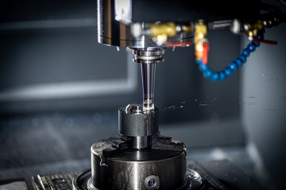
A reference flat or notch is then ground into the ingot to give the wafer a crystallographic orientation marker (typically ⟨100⟩ or ⟨111⟩) used downstream by lithography steppers, edge-inspection tools and chuck-alignment systems on the CMP polisher [S1][S5].
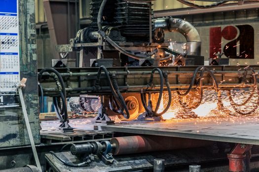
Slicing: ID Saw vs Diamond Wire Saw and Kerf Loss

Inner-diameter (ID) saws using a tensioned stainless-steel blade with bonded diamond grit were the workhorse for 100-200 mm wafers, cutting at blade speeds of 1500-3000 rpm and achieving kerf losses of 200-300 µm per slice [S1][S5].
Diamond wire saws have displaced ID saws above 200 mm, using a single wire of 0.10-0.18 mm diameter with fixed-abrasive diamond or loose-slurry SiC, running at 5-15 m/s and cutting kerf down to 100-130 µm while lifting throughput by roughly 2-3× on 300 mm ingots [S1][S3].
Wire-saw parameters drive two key wafer-level defects: saw marks (periodicity tied to wire diameter and feed) and wafer bow; managing wire vibration under 10 µm peak-to-peak is the practical gate for keeping as-sliced wafer warp below 30 µm on 300 mm parts [S3][S5].
Surface Prep: Lapping, Etching and Edge Profiling
Multi-wire-sliced wafers go through a double-side lapping step using a loose abrasive slurry of Al₂O₃ or SiC in the 5-15 µm grit range, removing 20-40 µm per side to bring TTV below 2 µm and erase saw damage to a depth of roughly 5-10 µm [S1][S5].
Wet chemical etching in mixed HF/HNO₃/CH₃COOH acids (typical ratios near 1:3:1 by volume) then strips the remaining saw-damaged layer, removing 10-20 µm per side and leaving a near-mirror but micro-rough surface at around 100-500 nm Ra [S1][S2].
Edge rounding follows, profiling the wafer rim to a radius of 200-300 µm on 300 mm parts to limit edge chipping during handling and to suppress slip-line generation during high-temperature CMOS well drives; this is the same edge-engineering logic called out in any V-process line discussion where rim geometry drives downstream yield [S1][S5].
Polishing: Single-Side CMP, Double-Side CMP and Final Clean
Stock-removal polishing (sometimes called pre-polish) uses a softer pad (e.g. IC1000/Suba-IV stack) and a colloidal silica slurry at pH 10-11 to take the wafer from lapped finish to roughly 1-2 nm Ra, removing 5-15 µm per side [S1][S5].
Final chemical-mechanical polishing (CMP) on a softer polymeric pad with diluted colloidal silica (SiO₂ particles 50-100 nm, 1-5 wt%) drives surface roughness to 0.1-0.3 nm Ra and near-zero haze below 0.3 ppm on a 300 mm wafer, with removal kept under 1 µm to protect the surface-denuded zone [S1][S2][S3].
Final cleaning sequences typically combine RCA-1 (NH₄OH/H₂O₂/H₂O, ~70 °C) and RCA-2 (HCl/H₂O₂/H₂O, ~70 °C) with megasonic-assisted rinsing to bring particle adders to fewer than 10 at ≥90 nm on a 300 mm wafer, the practical release gate for device-line handoff [S1][S5].
SiC and Specialty Substrates: Polishing Time Compression
For SiC power wafers, a three-step slurryless electrochemical mechanical polishing (ECMP) flow has been reported to reach atomically smooth surfaces from as-sliced 4H-SiC in under 2 h total, a meaningful compression versus the 6-8 h baseline of conventional slurry CMP on SiC [S4].
The same SiC polishing logic links to the silicon nitride and silicon-steel encyclopedia entries when selecting dielectric or magnetic substrates that share wafer-level flatness and roughness budgets, even though the chemistry is not interchangeable [S4].
Because SiC is roughly twice as hard as silicon in the Vickers sense, conventional Si polishing slurries underperform on SiC; the slurryless ECMP route replaces abrasive removal with an anodic oxide softened by a soft pad, which is the main mechanism behind the time reduction [S4].
Spec Snapshot for Process Engineers: 300 mm Prime Wafer Gate

On a 300 mm prime wafer the typical 2026 spec envelope is: diameter 300.0 ± 0.2 mm, thickness 775 ± 25 µm, TTV ≤ 3 µm, bow/warp ≤ 30 µm, surface roughness ≤ 0.2 nm Ra, and bulk resistivity 1-50 Ω·cm for CZ p-type ⟨100⟩ — numbers that line up with mainstream IC and additive manufacturing material reference stacks that consume high-purity silicon feedstocks [S2][S3].
Trade-offs between the four principal process options are tabulated below for direct comparison, with Czochralski as the default for CMOS, Float Zone for high-resistivity power, MCZ for low-striation memory, and slurryless ECMP as the emerging SiC-only branch.
Process options versus decision criteria (cost / resistivity / oxygen / wafer size readiness): CZ scores low cost, medium resistivity (1-100 Ω·cm), high oxygen (~10¹⁸ cm⁻³), mature to 300 mm; FZ scores high cost, high resistivity (>1 kΩ·cm), low oxygen (<10¹⁶ cm⁻³), practical to 200 mm; MCZ scores medium cost, medium resistivity, controlled oxygen, mature to 300 mm; slurryless ECMP on SiC scores medium cost, n/a (SiC bandgap), n/a, demonstrated on 150 mm 4H-SiC [S1][S2][S3][S4].
Limits, Failure Modes and What to Watch
COPs (crystal-originated particles) remain the leading yield-killer on advanced-node CZ wafers, driven by the bulk micro-defect density tied to cooling rate after growth; FZ is a structural mitigation but at 3-5× the wafer cost [S1][S2].
Wire-saw-induced micro-cracks and sub-surface damage (typically 1-3 µm deep on diamond-wire-sawn wafers) must be fully removed by lapping plus etching; under-etching is visible as hazy, low-breakdown-voltage wafers after CMP [S3][S5].
Trackable signals worth monitoring in the rest of 2026: 300 mm epitaxial-ready wafer ramp at the major merchant suppliers, slurryless ECMP qualification on 200 mm 4H-SiC production lines, and any shift in diamond-wire abrasive pricing that would reset kerf-loss assumptions below 100 µm [S3][S4].
For a process-engineer cross-check on related high-volume lines, the Aluminum Manufacturing Process: 2026 Line Stack, Alloy Flow and Finishing Snapshot and the Hydrogen fuel cell manufacturing process: stack build path, plate materials and 2026 articles cover comparable end-to-end line stacks where lapping, etching and CMP-style finishing also gate yield. The Multifunction Process Calibrator reference page is the relevant sanity check for the resistivity and temperature metrology that the CZ/FZ/MCZ gate above rests on.