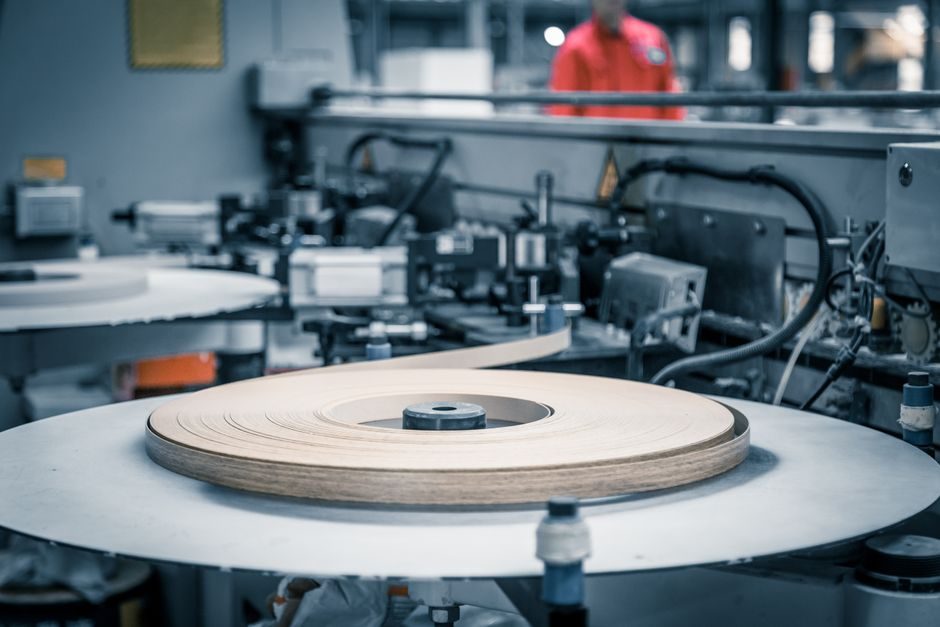
Seagate's Smart Manufacturing AI program — public since 2024 and expanded through 2026 — runs machine-vision defect classifiers and time-series models directly on wafer-fab lines, claiming factory-floor AI deployment at scale [S2].
The same closed-loop pattern (in-line metrology → model inference → recipe or robot retune) is now migrating to merchant 300 mm silicon wafer fabs, where the bottleneck processes — crystal growth, wire sawing, lapping, CMP — each have measurable defect and thickness signals that feed the same AI control loop. The 2026 build-out pairs legacy SECS/GEM host links with OPC-UA Pub/Sub and edge GPU inference, so MES/SCADA layers can trigger polishing-pad conditioning or dicing-blade dress cycles without operator intervention.
Process Bottlenecks That Drive Smart-Factory Spend
Silicon ingot-to-wafer conversion consumes most of the energy and yield budget in a fab: crystal growth, OD/ID grinding, multi-wire sawing, edge profiling, lapping, and chemical mechanical polishing each carry distinct failure modes that AI targets [S1].
Dicing alone is a documented yield hazard: chipping at die edges depends on blade bond, grit size, feed direction and wafer crystal orientation, with chipping size varying by wafer type and dicing direction in controlled scratching tests [S3]. Polishing is the downstream guard rail — chemical mechanical polishing (CMP) delivers the smooth, flat, particle-free surface that downstream lithography requires, and is described in the process literature as the dominant finishing step for implant-grade wafers [S5]. Smart-factory capital is concentrated at the three chokepoints where a sub-micron defect or a 1 % thickness drift is detectable in-line: sawing (kerf/chip), CMP (planarity, removal rate), and final clean (particle adders).
Closed-Loop Control Stack: Sensors, Models, and Robotics
The canonical 2026 closed-loop cell uses in-line optical defect inspection, spectroscopic thickness metrology, slurry pH/temperature sensors and acoustic-emission probes on the polisher, all feeding a real-time inference model that writes setpoints back to the tool PLC [S2].
Seagate's published deployment shows factory-floor AI running against high-volume drive production, with operators receiving predictions and prescriptive actions rather than raw alerts — the model layer, not the sensor layer, is the differentiating capital item [S2]. In a 300 mm wafer fab the equivalent stack is: (1) in-line interferometer for wafer thickness TTV; (2) white-light or laser-scatter particle counters post-CMP; (3) vision-based edge-chip detection after dicing; (4) a digital-twin model of the polisher head/pad that recomputes removal rate from slurry chemistry and pad age. The output is recipe retune commands written over SECS/GEM or OPC-UA, not a dashboard for a human.
Comparing the Main Process Steps on Smart-Factory Leverage

Sawing and CMP are the two highest-leverage points for closed-loop AI; crystal growth and edge grinding are lower-leverage because the dominant signals (defect density, edge roll-off) are slow to change and harder to actuate in real time [S1].
A practical comparison for a process engineer sizing 2026 automation capex: multi-wire sawing — fast feedback, single actuator (wire feed & tension), high defect-mode variety, strong AI case; CMP — continuous slurry chemistry signal, pad-wear actuation, high-yield case; lapping — slower drift, fewer sensors, moderate case; edge grinding — discrete, infrequent adjustments, weak AI case; final clean — particle-adders dominate, AI mostly predictive maintenance. The bias is clear: invest in the steps where the actuator response time is shorter than the defect formation time, and where the metrology is already in-line rather than at-line.
Standards and Interfaces That Govern the Stack
SEMI E84, E87 and the SECS/GEM HSMS family remain the binding host-to-tool interface inside a 300 mm fab; OPC-UA Pub/Sub is the layer above that, carrying model output to the MES and to the edge inference node [S2].
For the AI layer itself, IEEE 2934 provides a working framework for industrial AI system lifecycle, and IEC 62443 zones the OT network so the inference engine cannot be weaponised against the tool PLC. Functional safety on robot cells around the wafer handler follows ISO 10218 and ISO/TS 15066 for collaborative zones, with risk assessment per ISO 12100. The 2026 reference architecture sits on these rather than replacing them — smart-factory rollout is an integration problem, not a standards problem.
What Smart Manufacturing Is For, and Where It Is Not

Smart-manufacturing AI pays back fastest on lines that already run 24/7 with stable recipes and abundant historical WIP data; it pays back slowly on R&D or pilot lines where the process itself is changing weekly [S2].
For a 300 mm merchant wafer fab the case is strong: the product (prime polished wafer) is stable, the processes are mature, and the defect taxonomy is well understood [S5]. For a compound-semiconductor or SiC pilot line the same stack is overkill — the bottleneck is crystal yield, not metrology density, and AI on top of an unstable process amplifies noise. The selection rule: deploy smart-manufacturing AI only when recipe variance, not process discovery, is the dominant cost driver.
Failure Modes and Engineering Constraints
The most common 2026 rollout failure is sensor-to-model latency drift: a metrology tool that updates every 5 s cannot feed a polishing model whose actuator response is 200 ms, so the closed loop oscillates instead of converging [S2].
The second is data-labeling debt — vision-based edge-chip classifiers need labelled chip images, and without a curated set the false-reject rate climbs until operators stop trusting the system. The third is robot safety certification around wet benches and CMP tools, where the cleanroom envelope and the safety-rated monitored stop must coexist. Engineers should expect to spend as much capex on data infrastructure (label stores, model registry, edge GPU racks) as on the tool sensors themselves.
Sourcing and the 2026 Vendor Map
Smart-factory capital for wafer fabs in 2026 splits across three buyer groups: metrology OEMs (KLA, Onto, Hitachi High-Tech) for in-line defect and thickness tools, automation vendors (Applied Materials, TEL, Lam) for recipe-control integration, and edge-AI platform vendors selling the inference layer [S2].
Seagate's own deployment — vertical integration from drive media to AI stack — is the cleanest public reference for what an in-house smart-factory build looks like at scale, and is the template merchant wafer makers are now copying [S2]. The two watch signals for the next two quarters are: (1) published OPC-UA Pub/Sub reference configurations at the SEMI Standards meetings, and (2) any new IEC 62443-3-2 zone certifications on fab OT networks. Both are public, datable, and the cleanest leading indicators of where the 2026 wafer-fab smart-manufacturing capex is going. For the upstream process stack itself, the Silicon Wafer Manufacturing Process: 2026 Line Stack, Crystal Growth and CMP Gate reference is the companion read on where AI plugs into the line, and silicon carbide is the relevant next process node for power-device fabs that share much of the same metrology. The 2026 build pattern also borrows freely from smart camera inspection stacks proven in display and PV fabs, and the polishing-pad wear signals feed the same silicon nitride and silicon steel tooling suppliers who already ship into automotive lines — a useful procurement cross-check when qualifying dual-use metrology vendors.