Taiwan and South Korea together account for the majority of advanced-node silicon that ends up inside every laptop, server and pressure transmitter controller, with mainland China closing the gap on mature nodes and the United States rebuilding domestic front-end capacity under the CHIPS Act framework [S1].
For a process engineer reading a bill of materials, "where was the silicon made" now tracks to three coordinates: the wafer fab country, the process node class (3 nm / 5 nm / 7 nm vs 28 nm / 40 nm / 65 nm / 90 nm mature), and the back-end assembly/test country — usually Malaysia, Vietnam, mainland China or the Philippines [S2].
Front-End Wafer Capacity by Country: 2026 Snapshot
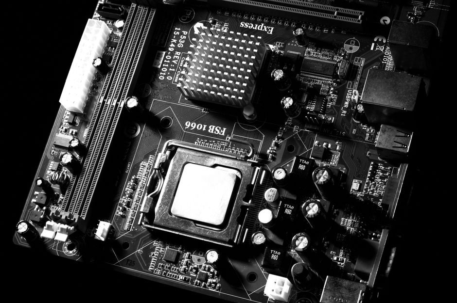
TSMC in Taiwan is the single largest contributor to leading-edge logic, operating multiple 3 nm and 5 nm fabs at full utilization and a parallel 2 nm risk-production line in Hsinchu, with 7 nm and 16 nm still absorbing automotive, AI accelerator and industrial controller demand [S1]. Samsung Foundry in South Korea runs 4 nm and 5 nm GAA lines at Pyeongtaek and produces 8 nm / 14 nm derivative nodes for image sensors and mobile SoCs. Intel's U.S. fabs (Arizona, Oregon, Ohio in build-out) anchor domestic capacity, with Intel 18A and Intel 3 serving client and server servo motor drive controller markets. GlobalFoundries (US/Germany/Singapore) and UMC (Taiwan) hold a large share of the 12 nm to 22 nm specialty range used in industrial MCUs, while SMIC and Hua Hong in mainland China lead mature-node output at 28 nm / 40 nm / 65 nm / 90 nm — the node band that feeds automotive-grade MCUs, PLC logic and a large slice of flow meter transmitter ASICs [S2][S3].
Mature vs Leading-Edge: Where Each Country Sits
The split between leading-edge and mature capacity is the most useful cut for sourcing engineers. Leading-edge (3 nm / 5 nm / 4 nm) production is effectively a three-country oligopoly: Taiwan, South Korea and the United States, with TSMC holding the dominant share and Samsung a distant second. Mature nodes (28 nm and above) are far more distributed: mainland China is the largest contributor by wafer count, followed by Taiwan, South Korea, the United States, Japan (Renesas, Kioxia adjacent fabs) and Europe (GF Dresden, STMicroelectronics Crolles). For a 32-bit industrial MCU specified into a pressure sensor signal chain, the die almost always traces back to a 40 nm or 90 nm fab in one of those geographies [S1][S2].
Back-End Assembly, Test and Package Geography
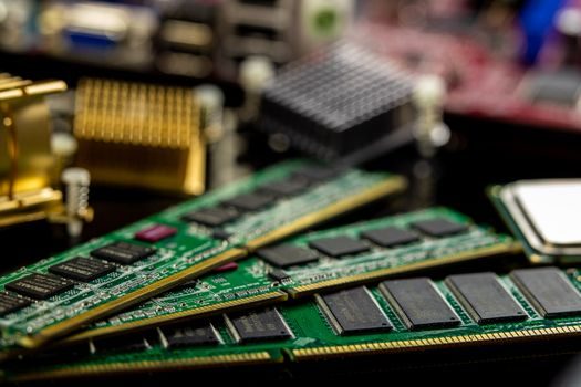
Even when the wafer comes from Taiwan or South Korea, the package is finished elsewhere. ASE, Amkor and JCET operate OSAT (Outsourced Semiconductor Assembly and Test) sites across Malaysia (Penang, Kulim), Vietnam (Hanoi, Da Nang), mainland China (Shanghai, Suzhou, Shenzhen), the Philippines (Laguna) and South Korea. CoWoS (Chip-on-Wafer-on-Substrate) advanced packaging for AI accelerators is bottlenecked almost entirely in Taiwan at TSMC, which is why a single 2.5-D package can sit on a six-to-eight month lead time [S1].
How to Use This Map When You Source an Industrial CPU
For a spec cut on a PLC CPU or a pressure transmitter MCPU module, the decision tree is short: (1) confirm the process node requirement (mature 28-90 nm is widely available from multiple geographies; sub-7 nm is Taiwan/US/Korea only); (2) confirm the package type (advanced 2.5-D packages constrain to Taiwan; standard QFP/BGA is open globally); (3) confirm the operating temperature grade — industrial -40 °C to +85 °C devices are typically qualified at 28 nm-40 nm mature nodes, not 3 nm; (4) confirm the qualification regime (AEC-Q100 for automotive, IEC 60079-x for hazardous-area industrial use, JEDEC for commercial). A sourcing engineer who locks these four inputs first avoids most 2026 lead-time surprises [S2].
Comparison: Major Producing Countries on 2026 Selection Criteria
Compared head-to-head, the four producing countries rank very differently. Taiwan: leading-edge share dominant, mature share high, lead times on 5 nm long (often 6+ months), geopolitical concentration risk. South Korea: strong on memory and foundry, second-source to TSMC on leading-edge, mature-node capacity moderate. Mainland China: dominant on 28 nm and above by wafer count, no access to EUV leading-edge, lead times on mature nodes short (typically 4-8 weeks), but U.S. export-control and entity-list overlap a real risk. United States: rebuilding on Intel 18A and GF, strong in defence and aerospace grades, capacity for industrial mature nodes moderate, lead times shorter for domestic buyers. For a flow meter or industrial valve controller specified to IEC 60079-x, mature-node mainland-China or Taiwan fabs are the practical default; for AI edge controllers needing sub-7 nm, Taiwan is still the only high-volume source [S1][S3].
Trackable Signals for the Rest of 2026
Two signals worth watching for the second half of 2026: TSMC's Arizona Fab 2 ramp is scheduled to bring additional 3 nm / 4 nm equivalent wafers into U.S. inventory in H2, and mainland China's domestic DUV multi-patterning work at SMIC continues to push effective 5 nm-class output, though at lower yield than TSMC N5. Industrial buyers with a six-to-twelve month forecast window should pin the fab country on every CPU datasheet, and treat mature-node China-sourced parts as a dual-source hedge against any single Taiwan fab disruption. See also this CNC machine supply chain 2026 review for how the same capacity-discipline approach applies to machine tools, and this mining equipment supply map for downstream lead-time risk patterns that mirror CPU fab concentration. [S1]