LED manufacturing is a two-stage chain: the epitaxial (epi) wafer line that grows the GaN/InGaN crystal layer on a substrate, and the back-end chip-process-and-package line that lithographs, dices and encapsulates the die into a usable light source [S3].
The choice of substrate — sapphire (Al₂O₃), silicon carbide (SiC) or silicon (Si) — sets wafer diameter, defect density, thermal conductivity and downstream cost; GaN-on-SiC gives the highest thermal conductivity and is the historical premium choice for high-brightness white and high-power applications, while GaN-on-sapphire dominates general lighting and display backlights [S3][S4].
Substrate Selection: Sapphire vs SiC vs Silicon
GaN-on-sapphire remains the workhorse of general lighting because 4-inch and 6-inch sapphire wafers are widely available, lattice-mismatch defects are managed with buffer layers, and the substrate is electrically insulating — which simplifies device isolation [S3]. The trade-off is thermal conductivity of roughly 23–25 W/(m·K) for sapphire at 300 K, which forces package-level heatsinking for high-current white LEDs.
GaN-on-SiC delivers thermal conductivity around 370–490 W/(m·K) for 4H-SiC, allowing higher current density per mm² of chip and longer lumen maintenance at high drive currents — a key reason it is used in projection, automotive headlamp and specialty lighting [S3]. ALLOS has separately demonstrated 200 mm GaN-on-Si epi wafers aimed at Micro LED display production, leveraging 200 mm Si CMOS lines for cost-down [S1].
GaN-on-Si is the cost-down path: Si wafers scale beyond 200 mm and integrate with mainstream semiconductor fabs, but the large thermal-expansion mismatch between GaN and Si (≈5.6 × 10⁻⁶/K vs ≈2.6 × 10⁻⁶/K) requires strain-engineered buffer stacks, and the path is still gated by yield and wavelength-uniformity challenges for high-end display use [S1].
Epitaxy and the MOCVD Workhorse
The active light-emitting layer is grown by Metal-Organic Chemical Vapor Deposition (MOCVD): trimethylgallium (TMGa), trimethylindium (TMIn) and ammonia (NH₃) react on the heated substrate, with InGaN multi-quantum-well (MQW) stacks emitting in the blue and green [S3]. Wavelength control comes from indium fraction in the well and well thickness; a 2–3 nm InGaN well shifted in indium content moves emission across roughly 450–530 nm.
MOCVD reactor throughput is a direct lever on cost: a single modern reactor can process a batch of 42×2-inch equivalents or run 6-inch wafers in a planetary or close-coupled showerhead configuration, with run durations typically 2–4 hours per MQW stack [S3]. For Micro LED display production, MOCVD wavelength uniformity across the wafer must hold within ±1 nm at 450 nm; ALLOS positions its GaN-on-Si epi specifically against that uniformity target [S1].
After epi, the GaN-on-SiC and GaN-on-sapphire path requires a laser-lift-off (LLO) or thinning step to expose the n-GaN contact for vertical-current devices — a process step that adds yield risk on thin wafers below 100 µm [S3].
Chip Process: Lithography, Mesa Etch and Electrodes
Standard LED chip fab starts with a p-GaN top contact (typically Ni/Au or indium-tin-oxide for current spreading), followed by photolithography and inductively-coupled-plasma (ICP) mesa etching down to n-GaN to define individual pixels, then n-contact deposition (Ti/Al) and annealing at 500–600 °C in N₂ [S3]. A typical blue LED chip die size for general lighting sits in the 200 µm × 200 µm to 1 mm × 1 mm range, while Micro LED display dies drop to 1–10 µm per pixel [S1].
For a white LED, the blue die is paired with a cerium-doped yttrium aluminum garnet (YAG:Ce) phosphor — either conformal-coated on the chip or remote-phosphor in the package — that down-converts a portion of the blue emission to broad yellow, producing white light with correlated color temperature (CCT) tunable by phosphor ratio [S3][S4].
Sorting (or "binning") follows: production wafers are tested for forward voltage (Vf), dominant wavelength (λd), and luminous flux (Φv), then grouped into ANSI bins; typical Vf for a 1 mm² blue die sits at 2.8–3.4 V at 350 mA, with λd held within ±2.5 nm for tight display backlight use [S3].
Packaging: From SMD 2835 to COB and CSP
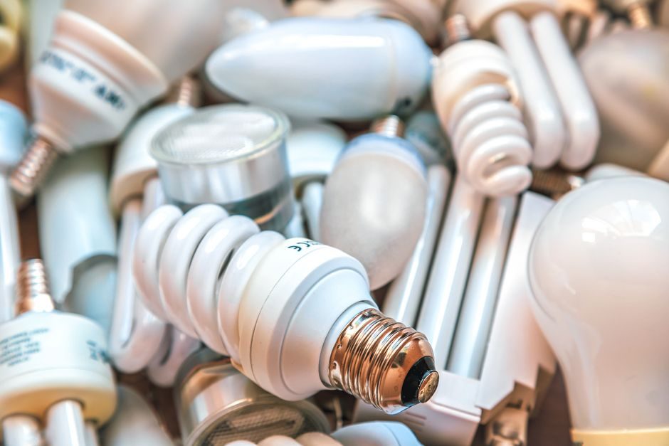
Package architecture has moved from through-hole 5 mm radial epoxy packages in the 1970s–1990s to surface-mount-device (SMD) types — 3528, 3014, 2835, 3030 — then to chip-on-board (COB) arrays for high-power downlights and streetlights, and most recently to chip-scale-package (CSP) LEDs with sub-150 µm light-emitting surfaces and zero-packaging-volume per lumen [S3][S4].
Junction temperature rise ΔTj is then ΔTj = Vf × If × Rth_j-c plus ambient; the same die spec'd in a CSP versus a plastic-lead 2835 will run 15–25 °C cooler at identical drive current.
Driver Topology and the Mains Interface
LEDs are current-driven, not voltage-driven; a small Vf shift across temperature and bin translates to large current excursions on a constant-voltage supply, so a constant-current driver is the baseline requirement [S3]. For mains-input white fixtures, two topologies dominate: a single-stage flyback with primary-side regulation (PSR) for sub-50 W retrofit bulbs, and a two-stage PFC + LLC or PFC + flyback for higher-power commercial luminaires, with power factor corrected to >0.9 to meet common utility standards [S3][S4].
Dimming comes in three flavors: analog 0–10 V, triac leading-edge phase-cut (used in residential retrofit), and digital addressable lighting interfaces (DALI-2, Zigbee, Casambi) — each adds BOM cost and demands different driver-side circuitry, and the wrong pairing of triac dimmer and LED driver is the most common field complaint for flicker and audible noise [S3].
For specialty sources such as the UVC (200–280 nm) AlGaN-based emitters used in sterilization, water/air purification and medical hygiene, drivers must also handle the lower Vf of deep-UV dies (typically 5–7 V at 100–350 mA) and provide tighter current regulation, since UVC output scales near-linearly with current and small current drift directly maps to sterilization-dose error [S2].
What LED Production Is and Is Not For
LED production is for: general illumination where efficacy >120 lm/W, lifetime >25,000 h and CCT control matter; display backlights where wavelength binning ±2.5 nm and uniformity across the panel drive panel-quality yield; UV sterilization/curing where specific 265 nm or 395 nm peak output is needed; and Micro LED micro-displays where the small die size forces wafer-level mass transfer [S1][S2][S3].
It is NOT for: applications where the device is expected to run above its rated Tj without derating, where a single-color high-power laser source is required (laser diodes are a different device family), or where the supply chain cannot tolerate tight binning — the cost of a "white-LED retrofit" rises sharply when 3-step MacAdam SDCM bins are specified instead of 7-step [S3][S4].
Side-by-Side: The Three Substrate Paths
On four decision criteria — cost per wafer, thermal conductivity, wavelength uniformity for display use, and 6-/8-inch scalability — the three paths line up as follows [S1][S3]:
1) GaN-on-sapphire: lowest cost per wafer area, ~23 W/(m·K), wavelength uniformity held within typical display bin limits, scalable to 6-inch widely, 8-inch in development.
2) GaN-on-SiC: highest cost per wafer area, ~370 W/(m·K), tightest wavelength uniformity on small wafer area, 4-inch and 6-inch production lines, 8-inch not standard.
3) GaN-on-Si (Micro LED focus): low-cost silicon wafer at 200 mm+, ~150 W/(m·K) for Si substrate, wavelength uniformity still being engineered for display-grade output, scales to 200 mm+ via CMOS fabs [S1].
Limits, Failure Modes and Standards
The dominant reliability failure modes for white LEDs are: phosphor thermal degradation at high Tj (>120 °C), silicone encapsulant yellowing and cracking under thermal-cycling, and silver-mirror migration at the p-contact under high humidity — all three are accelerated at Tj above manufacturer ratings [S3][S4]. For automotive exterior lighting, the relevant qualification flow is AEC-Q102 (LED-specific), with stress conditions including wet-hot thermal cycling and high-temperature operating life (HTOL) at rated current.
Standards governing measurement and safety include: IES LM-80-15 for lumen-maintenance testing (10,000 h minimum reporting window for LM-80-15 with TM-21-19 projection); IEC 62471 for photobiological safety classification of lamps (Risk Group 0–3); and IEC 62031 / UL 8750 for safety of LED modules and light engines. Color rendering is reported as CRI Ra (0–100) and more recently as TM-30 Rf (fidelity) and Rg (gamut), with premium general-lighting LEDs hitting Ra >90 and Rf >90.
For UV sterilization, IEC 62471 places 200–315 nm emitters in higher risk groups without enclosure, and most commercial UVC products are sold only into fixed-installation markets because of skin/eye hazard — making driver interlock and presence-sensing a hard design requirement, not an option [S2].
Adjacent Process Lines Worth Tracking
The same MOCVD epitaxy and wafer-fab lines that feed LED production also feed the GaN power-device line; the semiconductor spot-price tracker for MOSFET and IGBT quotations is a useful cross-read on shared 6-inch/8-inch SiC and GaN-on-Si capacity, which in turn gates LED wafer supply. [S1]
For high-power lighting tied to solar-plus-storage street and industrial sites, the top solar panel companies pricing bands and installer coverage reference is the natural downstream spec context for an LED module designed to run off DC bus or battery storage.
Process engineers tracking sub-system sourcing for LED packaging lines — die bonders, wire bonders, silicone encapsulant dispensers — will find shared sourcing dynamics with the additive manufacturing 2026 serial production and MRO reference, since both lines depend on the same mid-volume SMT-class automation tier.
Looking forward, the next trackable signals in LED production are: 200 mm GaN-on-Si Micro LED epi yield ramp at display fabs [S1], LM-80-15 + TM-21-19 reports from CSP and COB vendors crossing 50,000 h extrapolation, and any 8-inch GaN-on-sapphire MOCVD reactor announcements from the major equipment makers — each will materially shift cost-per-lumen and the substrate split.
For component-level specifications, see pressure transmitter, flow meter, and industrial valve.