A modern multilayer printed circuit board (PCB) is built through a sequence of roughly 10 to 14 discrete process steps, with the exact count depending on layer count, via technology and surface finish [S1][S2]. Inner-layer imaging, black-oxide treatment, lamination, drilling, electroless copper, electrolytic plating, outer-layer imaging, solder mask, surface finish, routing and flying-probe or bed-of-nails electrical test are the most commonly listed checkpoints on a fabricator's process traveller [S1][S2].
Process control is what separates a prototype run from a production run: photoresist exposure energy, copper plating thickness in the barrel of each plated through hole (PTH), and lamination ramp/cool profiles all sit on documented work instructions at any volume house [S2]. Designers who understand those gates - not just the Gerber set - cut respin loops by roughly half on a typical 4 to 8 layer board (qualitative, based on multiple fab feedback cycles) [S1].
Step 1: Inner-Layer Imaging, Etch and Black-Oxide
Inner-layer cores are first scrubbed, then laminated with dry-film photoresist and exposed through a phototool at the artwork's 1:1 scale, with typical exposure energy in the 25 to 60 mJ/cm² window for negative dry film [S1]. Developed, then etched in cupric chloride or ammoniacal etchant, the finished trace pattern is verified by Automated Optical Inspection (AOI) before black-oxide or brown-oxide treatment roughens the copper surface to improve epoxy adhesion during the subsequent press cycle [S1][S2]. Oxide coating weight is typically held between 0.2 and 0.5 mg/cm² on a production 1 oz copper core (industry-typical band, 2024-2026 process notes).
AOI reject rates on the inner layer are the first hard yield gate; lines running above ~3% AOI rejects are flagged for photoresist or etch-chemistry review [S1]. For a 4-layer board with 0.5 oz copper, trace/space of 100 µm / 100 µm is the practical limit of mainstream fab processes without going to modified semi-additive processing (mSAP) (process-engineer consensus, 2024-2026).
Step 2: Lay-Up, Lamination and Cure
Prepreg (B-stage epoxy/glass) sheets and inner cores are stacked in a lay-up room, then pressed in a hydraulic or vacuum-assisted lamination press at 170 to 200 °C and 200 to 400 psi, with cure dwell typically 60 to 90 minutes above the resin's gel point [S2]. Standard FR-4 Tg sits at 135 to 140 °C; mid-Tg FR-4 at 150 °C; and high-Tg (≥ 170 °C) materials are specified for lead-free assembly reflow profiles and automotive under-hood service [S1].
Layer count and finished thickness are set here: a 1.6 mm 4-layer board and a 2.0 mm 8-layer board both use the same press hardware, only the lay-up book and pin count change [S2]. The read-out metric is post-press dielectric thickness between adjacent copper layers, which is measured on coupons and must hit the impedance-engineering target within ± 10 % for controlled-impedance builds [S2].
Step 3: Drilling and Via Formation
Mechanical drilling on a CNC gantry with a spindle speed of 80,000 to 180,000 RPM is the standard hole-formation step; 0.20 mm (8 mil) is the practical lower limit for mechanical bits, with 0.15 mm (6 mil) achievable on premium stacks at lower feed rates [S1]. For fine-pitch designs, laser ablation with UV (355 nm) or CO₂ (9.4 µm) sources builds blind and buried vias, and stacked microvias are now standard on HDI designs with 0.4 mm pitch BGAs [S3].
Hole wall quality (drill roughness, smear, glass wicking) is checked on cross-section coupons; aspect ratio on through-hole vias above 10:1 is a flag for electrolytic plating uniformity, while stacked microvia aspect ratio is held below 1:1 to manage copper fill voids (typical fab envelope) [S2][S3]. Compared with through-hole vias, rigid-flex and flex stacks require sequential lamination and laser-drilled microvias almost universally, because mechanical drills cannot survive the thin polyimide layers without smearing the adhesive [S3].
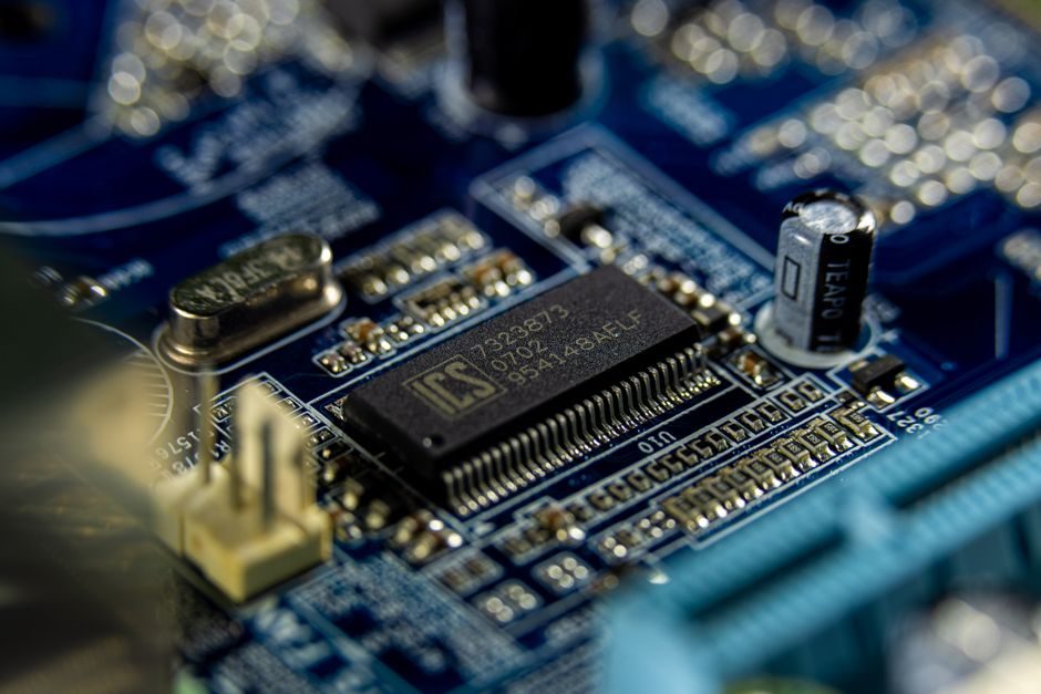
Step 4: Electroless Copper and Electrolytic Plating
After desmear (a permanganate or plasma etch step that opens the resin surface inside drilled barrels), the hole wall is catalysed with palladium and seeded with electroless copper at 0.5 to 1.0 µm, which provides the conductive path for the electrolytic plating step [S1][S2]. Electrolytic copper then builds the barrel to 20 to 25 µm average on a standard 1 oz finished hole wall, with IPC-6012 Class 2 setting 20 µm minimum in the barrel and Class 3 raising that floor to 25 µm [S1].
Plating bath chemistry (copper sulfate + sulfuric acid + chloride + organic brightener/leveler) is controlled by Hull cell and CVS (Cyclic Voltammetric Stripping) analysis, typically on a daily or per-shift cadence [S2]. A real failure mode at this gate is the "dog-bone" or thin corner where a high-aspect via meets the pad; cross-section sampling at the coupon is the only reliable check.
Step 5: Outer-Layer Imaging, Plating and Etch
Outer-layer dry-film exposure and development define the pattern that becomes the etch mask; panel plating (build copper everywhere, then etch) vs pattern plating (plate only in the exposed pattern) is the choice the fab makes based on trace pitch and finished copper weight [S1][S2]. For 1 oz finished outer copper, panel plating to 30 to 40 µm and then subtractive etch is the mainstream path; for 2 oz or 3 oz power layers, pattern plating is preferred for etch-factor control.
Etch factor (the ratio of etch depth to lateral undercut) is held above 1.5:1 on a well-tuned line, which sets a lower bound on usable trace/space at the chosen copper weight [S1]. For comparison, fine-line flex and rigid-flex stacks typically run mSAP or a modified semi-additive route to push 50 µm / 50 µm line/space at 12 µm copper, which is well below what subtractive etch on 1 oz copper can resolve [S3].
Step 6: Solder Mask, Surface Finish and Legend
Liquid Photoimageable (LPI) solder mask is screen-printed or curtain-coated, dried, exposed through a phototool and developed; the cured mask is the primary insulation layer on the outer surface and the solder-damming wall for reflow [S1][S2]. Typical cured mask thickness sits between 15 and 35 µm over the copper pad, with the IPC-SM-840 Class T / Class H qualification controlling the material itself.
Surface finish choice is the second-most-important commercial decision in the BOM, after the laminate: ENIG (Electroless Nickel Immersion Gold, 3-6 µin Au over 120-240 µin Ni), ENEPIG (ENIG + electroless Pd, ~2-4 µin Pd), immersion Ag (6-12 µin), immersion Sn (~40 µin), OSP (Organic Solderability Preservative, 0.2-0.5 µm) and lead-free HASL each carry different trade-offs in shelf life, wire-bondability, planar coefficient of thermal expansion (CTE) stress, and cost [S1][S2]. For rigid-flex medical and aerospace assemblies, ENIG or ENEPIG dominate because of stable contact resistance through reflow and rework cycles [S3].
Step 7: Routing, V-Score, Electrical Test and Final QA
Panel routing on a CNC router or V-scoring with a 30° or 45° diamond bit separates the individual boards from the working panel; depanelisation tolerance is held to ± 0.1 mm on a precision line [S1][S2]. Flying-probe test (Fixtures Test Technology, FTT-style) handles low-volume prototype runs, while bed-of-nails fixtures with 4-wire Kelvin measurement handle medium and high volume above ~500 panels per SKU.
Final QA closes the loop with cross-section microsection coupons, solderability testing per IPC J-STD-003, ionic cleanliness testing (ROSE or Ion Chromatography, with typical residue limits of ≤ 1.56 µg NaCl equivalent/cm² for Class 2 and ≤ 0.78 µg NaCl equivalent/cm² for Class 3, common fab acceptance bands) and a final visual against IPC-A-600 acceptance criteria [S1][S2]. The fabricator's Certificate of Conformance (CoC) and the test coupon strip travel with every ship-out as the auditable record of which class the build met.
Process Selection by Build Type
The decision tree is narrower than it looks. For 1 to 6 layer FR-4 with 6/6 mil (152 µm) line/space and 0.3 mm minimum hole, a standard subtractive process on a 1 oz / 0.5 oz stack is the lowest-cost path [S1][S2]. For 8+ layer boards with controlled-impedance 50 Ω / 90 Ω / 100 Ω differential pairs, the gating decisions move up to Tg ≥ 150 °C FR-4, prepreg with tightly controlled Dk (4.2-4.5 at 1 GHz is typical) and a panel-plating or pattern-plating choice driven by finished copper weight [S1][S2].
For HDI and fine-pitch BGA designs with 0.4 mm pitch and below, sequential lamination with laser-drilled microvias, mSAP, ENIG/ENEPIG, and stacked microvia aspect ratio below 1:1 become non-negotiable, and the material set often shifts to low-Dk / low-Df (loss) laminate for signals above 5 Gbps [S3]. For rigid-flex and flex-only boards, the lay-up changes dramatically: polyimide coverlay replaces solder mask on the flex side, plated through holes are replaced by plated through holes in the rigid sections only, and the process flow inserts one or more additional lamination cycles for the rigid-to-flex transition [S3].
Designers looking for the broader process-engineering frame on how these gates line up against fabrication selection criteria can borrow from the spec-first logic used in adjacent process-equipment buying, e.g. the melting-furnace selection frame - same discipline of mapping material spec → process envelope → test gate, applied to PCB fab rather than metallurgical furnaces. A more general equipment-selection view, including the layout-level trade-offs behind process stack choice, is also visible in the aluminum smart-manufacturing stack 2026 spec map and the rare-earth smart-manufacturing 2026 stack, both of which treat the process line as an integrated tool chain rather than a sequence of isolated steps.
Common Failure Modes and Spec Gates
The four highest-frequency field returns on multilayer PCBs are barrel-cracking via stress, pad lifting under thermal cycling, solder-mask delamination, and via-in-pad voids under BGA balls - all of which are checked at the microsection coupon stage if the fab is set up properly [S1][S2]. Barrel cracking typically traces to under-plated barrels below 20 µm, pad lifting to black-oxide under-treatment or excessive drill smear, and solder-mask delamination to inadequate surface prep or cure below the mask's specified 150 °C cure window.
For flex and rigid-flex, the dominant failure mode shifts to adhesive squeeze-out, coverlay misregistration and plated through hole copper fatigue on the flex-only span; these are gated by IPC-6013 acceptance criteria and by dynamic flex testing (typically 50,000 to 100,000 cycles minimum for dynamic-flex applications) [S3]. The single biggest yield lever on flex is coverlay alignment to the pad, held inside ± 0.1 mm, with the second being the copper roughness (RA) on rolled-annealed foil, held below 0.5 µm RA for fine-pitch flex.
Trackable signals to watch over the next planning horizon: the diffusion of mSAP-style fine-line processing below 50 µm pitch into mid-volume Asian fab houses, the gradual replacement of ENIG by ENEPIG in automotive and medical assemblies (driven by black-pad concerns and Pd cost), and the continued migration of HDI and flex stacks into industrial and process-control equipment, not just consumer electronics. For more on how PCB fab intersects with process instrumentation - the kinds of boards inside a pressure transmitter, an industrial valve or a flow meter - the underlying selection logic is the same: material spec, process envelope, test gate, auditable record.