IGBT smart manufacturing combines 12-inch wafer fab automation, AI-based in-line defect classification, and MES-level traceability to drive insulated-gate bipolar transistor (a BJT-MOS composite power device) module yields above 90% on automotive-grade lines [S1][S3].
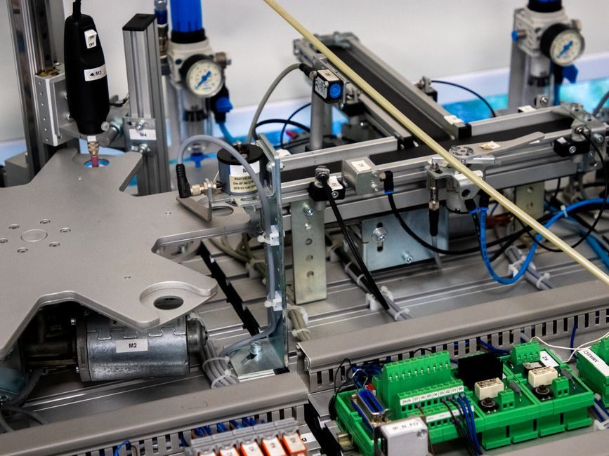
The scope is the discrete power-device back-end: thin-wafer dicing, backside metallization, wire/clip bonding, and module housing, all stitched to an industrial automation layer (Rockwell, Siemens, Beckhoff PLC families) and a manufacturing execution system that records every die's traceability code [S2].
Definition and Stack Layers for IGBT Smart Manufacturing
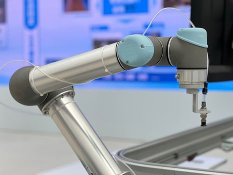
Smart manufacturing is the integration of IoT, AI, big-data analytics and cloud computing across every layer of the production process, turning a conventional fab into a self-monitoring, self-optimizing system [S1]. For IGBT, that translates into four physical layers: equipment (implanters, LPCVD, CMP, sputter, dicing saws, wire bonders, ultrasonic welders); instrumentation (smart cameras, flow meters, pressure transmitters on gas/liquid lines); edge compute (PLC + industrial PC running OPC UA over TSN); and enterprise (MES, EAP, R&D EDA, supplier portal) [S2]. IGBT is itself a BJT-MOS composite, full-controlled, voltage-driven power semiconductor, so its fab requires tight control of minority-carrier lifetime, gate-oxide thickness and backside thinning tolerances [S3].
On top of these four layers, the data fabric typically runs ISA-95-style hierarchical models, with OPC UA Pub/Sub on TSN as the field-level backbone. Smart valves, smart meters and smart camera nodes publish directly to the MES broker; recipe download, lot tracking and golden-batch comparison run as MES services. SourceBySpec's reference on smart meters and pressure transmitters maps the field device side of this stack.
Selection Criteria: Which Processes Are Worth Closing the Loop
Not every step pays back the same when closed-loopped. High-value targets in IGBT lines are thin-wafer dicing (kerf loss < 50 µm, die strength > 200 MPa), backside metallization (Ti/Ni/Ag stack, thickness uniformity ±5%), ultrasonic welding of wire bonds (pull strength > 6 g for 200 µm Al wire), and final test (Vce(sat), Eon/Eoff, thermal resistance Rth(j-c)) [S1][S3].
Selection gate, in priority order: (1) defect Pareto contribution, (2) sensor feasibility (non-contact optical, X-ray, acoustic), (3) controller latency budget (sub-10 ms for motion, 100 ms for thermal), (4) data model fit into the existing ISA-95 B2MML schema, and (5) capex/opex ROI under 24 months. A practical rule: if a step contributes more than 15% of line yield loss and has a measurable in-line sensor, close it; otherwise run it in advisory mode. The smart camera class dominates because AI-vision defect classification is the highest-leverage non-contact sensor for both wafer and module stages.
Who It Is For vs Who It Is Not For

IGBT smart manufacturing is for: Tier-1 power-module makers running 6-inch or 8-inch legacy lines, IDMs and foundries converting to 12-inch thin-wafer processing, and automotive-qualified IGBT module pack houses serving EV traction inverters. It is also for OSAT-style back-end lines that need per-die traceability under AQG-324 / VW 80000 / AEC-Q101 regimes [S3].
It is not for: low-volume custom IGBT die shops (lots under 500 wafers/month), rectifier-grade thyristor lines where process variance is tolerated, or R&D fabs without a stable recipe baseline. Trying to bolt AI yield analytics onto a process with Cp/Cpk under 1.0 wastes money; stabilize the line first, then close the loop. The same logic shows up in silicon wafer smart manufacturing, where CMP closed-loop is gated on a stable slurry and pad baseline.
Comparison of Main Automation Tiers on IGBT Lines
Three automation tiers compete in the IGBT back-end, and the right pick is set by volume, mix and audit regime. Tier 1 is PLC + SCADA + MES (typical for module assembly, 50-200 ms loop, ISA-95 B2MML, capex in the low single-digit $M). Tier 2 is PC-based control + OPC UA over TSN + edge AI (sub-10 ms motion, AI-vision inline defect classification, $M-scale). Tier 3 is full lights-out with autonomous material handling, AMHS-style overhead transport, and 100% in-line X-ray / acoustic inspection ($10M+ capex) [S1][S2].
Decision criteria for picking a tier, with typical bands:
1) Throughput need: under 5,000 wafers/month per line points to Tier 1; 5,000-20,000 to Tier 2; over 20,000 to Tier 3.
2) Automotive audit depth: AEC-Q / IATF 16949 / AQG-324 typically forces Tier 2 minimum, because per-die traceability and e-diagnostics data are non-negotiable.
3) Latency on critical loops: wire-bond force/displacement loop wants sub-1 ms, achievable only on Tier 2 or Tier 3 with EtherCAT or TSN; Tier 1 PLC scan times are too slow.
4) Data model: Tier 1 typically supports ISA-95 + OPC UA classic; Tier 2 adds OPC UA Pub/Sub and MQTT; Tier 3 adds digital twin + R&D EDA loop-back.
Real Use Cases in IGBT Fabs
CMP closed-loop on backside thinning: a flow meter + turbidity sensor on the slurry loop drives a removal-rate model; the controller adjusts downforce in real time to keep total thickness variation under ±2 µm across a 200 mm wafer. Closed-loop CMP has become a baseline expectation on 12-inch power-device lines, with similar architectures detailed in silicon wafer smart manufacturing.
Module housing and ultrasonic welding: smart camera + laser profile + acoustic emission sensors verify weld stack height and bond footprint; rejects are auto-diverted and the recipe is auto-tuned every 50 bonds. The MES stores the per-module bond map for end-of-line traceability.
Final test data lake: dynamic Vce(sat), Eon/Eoff and thermal impedance Rth(j-c) per part are streamed into a time-series store, and a gradient-boosted yield model flags drifts against the golden batch within minutes rather than the next-day SPC review [S1][S2].
Limitations, Constraints and Failure Modes
Three constraints bite hardest. First, sensor drift in vacuum and plasma tools: optical emission and RF sensors need recalibration against a reference wafer, and drifting sensors quietly poison the training data of any AI model trained on top [S1]. Second, data-model fragmentation: OPC UA companion specs for power-device processes are still maturing, and many Tier 1 MES vendors do not yet expose the B2MML views that yield analytics need [S2]. Third, organizational: closed-loop control only works when the process engineer owns both the recipe and the controller setpoint; matrixed ownership creates 24-48 h decision lag that defeats the loop.
Failure modes to monitor: (a) AI model trained on a non-representative lot and then promoted globally; (b) MES-to-equipment handshake failing silently, causing recipes to be applied out of order; (c) OPC UA security misconfig on the field network opening the cell to unintended writes; (d) AMHS/robot interlocks in Tier 3 not being tested at the same cadence as the process tools. The smart valve positioner class of field device shares the same cyber-physical failure surface.
Standards, Sourcing and Trackable Signals

Standards touch the stack at multiple points: ISA-95 / B2MML for MES-EAP integration, OPC UA over TSN for field-level networking, SEMI E84 / E87 for equipment hand-off, AQG-324 for automotive power-module reliability, and IEC 60749 / AEC-Q101 for discrete device qualification. Safety on hydrogen and acid gas lines falls under IEC 60079-x / ATEX 2014/34/EU when the line is sited in Europe [S2].
Sourcing map, as of 2026-06-25: Tier 1 MES is dominated by the usual industrial-software majors; Tier 2 edge-AI and AI-vision come from a mix of industrial-automation incumbents and pure-play vision specialists; Tier 3 lights-out AMHS is still concentrated in semiconductor-grade suppliers with a thinner field of merchant vendors [S1][S2]. For fab planners reading a 2026 capex calendar, the realistic decision is usually a hybrid Tier 1 + Tier 2 stack with selective Tier 3 islands, not a top-down jump to full lights-out.
Trackable signals to watch over the next 6-12 months: (1) public announcements of 12-inch IGBT line ramp-ups in CN, JP, KR and DE, (2) updates to AQG-324 and the alignment of automotive IGBT module traceability requirements with EU battery passport rules, (3) OPC UA companion-spec coverage of power-device-specific process steps. The same closed-loop playbook also drives additive manufacturing material lines, so the same instrumentation and MES patterns reappear across discrete power devices, wafers and metal-AM, and cross-reads against industrial robot supply will tell you whether the AMHS side of Tier 3 is even buildable on schedule.